What Is a SerDes? Complete Guide to Meaning, Purpose, Architectures & Real-World Design
1. What is the meaning of SerDes?
1.1 Definition & Basics
SerDes stands for SERializer/DESerializer, a mainstream serial communication technology for Time Division Multiplexing (TDM) and Point-to-Point (P2P) connections. At the transmitter, multiple low-speed parallel signals are converted into high-speed serial signals. These signals traverse the transmission medium (fiber optic cable or copper wire), and at the receiver, the high-speed serial signals are reconverted into low-speed parallel signals. This point-to-point serial communication technology maximizes the channel capacity of the transmission medium, reduces the number of required transmission channels and device pins, increases signal speed, and significantly lowers communication costs.
With advancements in electronics technology, particularly in transmission interfaces, traditional parallel interfaces have reached a speed bottleneck. They are being replaced by faster serial interfaces, making SerDes technology—initially developed for fiber optic communications—the mainstream solution for high-speed serial interfaces. Serial interfaces primarily employ differential signal transmission technology, offering low power consumption, strong interference resistance, and high speed, with maximum transmission rates exceeding 10Gbps.
Before SerDes gained popularity, data between chips was transmitted via system-synchronous or source-synchronous parallel interfaces.
SerDes Advantages: Reduced I/O count, smaller packaging, fewer traces, and lower cost; effectively reduces electromagnetic interference, noise.
Crosstalk—SerDes Disadvantages: Higher system design complexity and the need for higher-performance channel materials.
Key technologies enabling higher speeds and bandwidths for SerDes include multiplexing, differential signaling, clock data recovery, and link equalization.
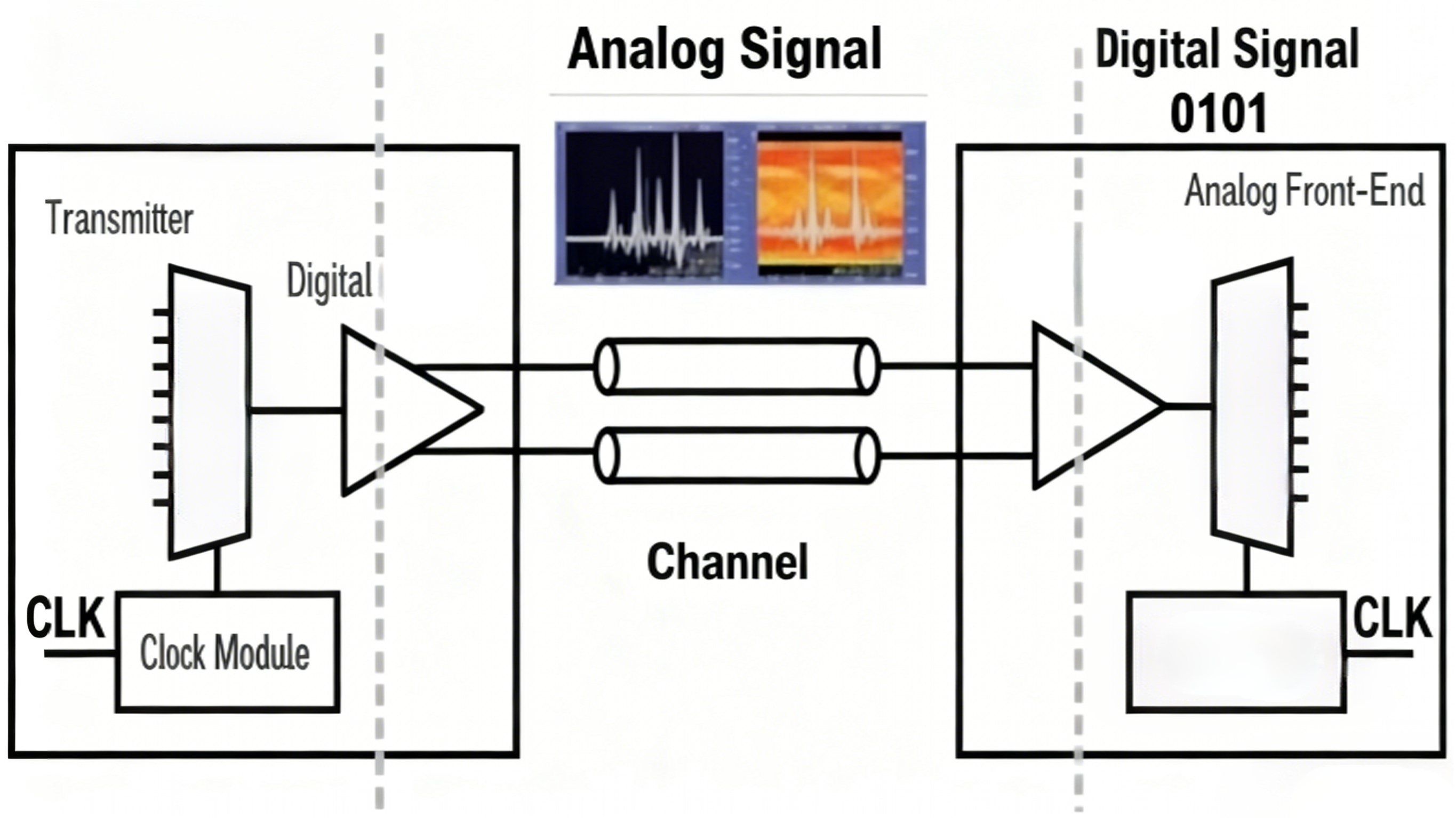
As shown in the diagram above, SerDes is a mixed-signal chip that operates in pairs.
1.2 SerDes vs. Interface Protocol
SerDes and interface protocols are closely related yet fundamentally distinct concepts.
Simply put
SerDes is a physical layer (PHY) technology—a "foundational hardware technology" or "core engine" enabling high-speed serial communication.
An interface protocol is a set of communication rules that defines a "complete communication standard," including electrical characteristics, data formats, link management, error handling, and more.
Their relationship can be analogized as:
SerDes is the engine and transmission of a car (providing core power and transmission).
Interface protocols are the complete traffic regulations and vehicle standards (including road signs, driving rules, licensing exams, etc., while also specifying emission standards engines must meet.
Specific interfaces like PCIe, SATA, and USB are like distinct vehicle models (e.g., SUVs, sports cars, trucks). They adhere to traffic rules (protocols) while utilizing engines (SerDes).
Below, we compare them in detail across several dimensions.
|
Dimension |
SerDes (Serializer/Deserializer) |
Interface Protocol |
|
Essence |
A type of hardware IP core or circuit |
A complete set of communication standards, specifications, and protocol stacks |
|
Function |
Parallel-to-serial conversion (Serializer) and serial-to-parallel conversion (Deserializer). The core function is to complete the serialization and deserialization of digital signals. |
Define the entire communication process: data packet structure, link training, traffic control, error checking, power consumption management, software interaction, etc. |
|
Layer |
Primarily operates within the electrical sublayer and logical coding sublayer of the physical layer (PHY). |
Covers the physical layer (PHY), data link layer, and even higher layers (such as the transaction layer). |
|
Focus |
Signal integrity, timing convergence, jitter, power consumption, bit error rate (BER). "How to reliably transmit 0s and 1s". |
Interoperability, compatibility, functional correctness, system performance. "What data to transmit and how to interact". |
|
Technical Core |
Clock Data Recovery (CDR), Pre-emphasis, Equalization, Eye Diagram, etc. |
Data packet format, link training state machine, acknowledgment/retransmission mechanism, virtual channels, enumeration process, etc. |
|
Dependency |
Does not depend on a specific protocol. A SerDes circuit can support multiple different protocols (such as PCIe or SATA) through configuration. |
Highly dependent on the physical layer, typically specifying or utilizing a specific SerDes technology to meet its physical layer requirements. |
|
Examples |
• Xilinx/AMD's GTY/GTM Transceiver • Intel's GPIO LVDS or AIB • Various SerDes IP cores |
• PCI Express (PCIe) • USB (3.2/4) • SATA/SAS • Ethernet • MIPI C/D - PHY |
1.3 Where SerDes Lives
(1) As an Integrated IP Core
This is the most common and mainstream form of SerDes. It is not a standalone chip but rather an intellectual property (IP) module integrated into a larger chip (such as an SoC, FPGA, GPU, or CPU) during the design phase.
Analogy: This is akin to a compressor already installed inside a large appliance (like a refrigerator). When you buy a fridge, you don't purchase the compressor separately; it is one of the core components, specifically designed to serve the refrigerator's overall functionality.
Specific Description
In ASICs or SoCs: Exists as complex macros or soft IP. For example, mobile processors (SoCs) integrate multiple MIPI D-PHY/C-PHY SerDes for connecting cameras and displays, and PCIe SerDes for high-speed data exchange. In FPGAs: Pre-hardened as complex IP on silicon for optimal performance. Examples include GTH/GTY transceivers in Xilinx/AMD UltraScale+ FPGAs, LVDS SERDES in Intel FPGAs, or hardened IP for PCIe. Soft IP implementations exist but typically offer inferior performance.
Features
High Performance, Low Latency: Direct integration within the chip minimizes interconnect routing to other components, enabling extremely high speeds with minimal power consumption and latency.
High Bandwidth Density: Dozens or even hundreds of SerDes channels can be integrated onto a single chip (e.g., high-end switch chips).
Cost-optimized: For mass production, the integrated solution eliminates additional chip, PCB area, packaging, and pin costs, resulting in lower overall expenses.
Low Power Consumption: On-chip interconnect power consumption is significantly lower than that of PCB traces driving signals between chips.
Limited flexibility: Once manufactured, the SerDes type, data rate, and protocol support are fixed and cannot be upgraded.
Application Scenarios
Computing chips: PCIe and DDR controller interfaces in CPUs and GPUs.
Mobile Platforms: MIPI and USB interfaces in mobile SoCs.
Network chips: Ethernet (1G/10G/100G...) SerDes in switch and router chips.
Storage controllers: SATA, SAS controllers.
FPGA: Nearly all mid-to-high-end FPGAs integrate multiple high-speed SerDes hard cores for implementing various protocols.
(2) As a standalone chip (Standalone Chip / PHY)
In this form, SerDes functions as a standalone, single-purpose physical layer (PHY) chip. It typically serves as a bridging or expansion device, connecting chips lacking high-speed serial interfaces to high-speed serial links.
Analogy: This is like an external compressor. If your old refrigerator's compressor fails, or you want to upgrade the cooling capacity of a small freezer, you can attach one externally.
Specific Description
Form Factor: A standalone chip, typically connected to the host controller via parallel buses (e.g., PCIe, SGMII, XAUI) or serial buses. Its function is highly specialized: primarily handling serial-to-parallel/parallel-to-serial conversion and physical layer signal processing, while protocol handling remains the responsibility of the host chip.
Features
High Flexibility: Adds high-speed connectivity (e.g., 10 Gigabit Ethernet, PCIe) to legacy or low-cost host chips lacking native high-speed interfaces (e.g., microcontrollers, entry-level FPGAs).
Upgrade and Bridging
Commonly used for protocol conversion or interface expansion, such as interface cards/chips converting PCIe to SATA or USB.
Performance Overhead: Data must exit the main chip, traverse the PCB to the SerDes chip, and undergo processing, introducing additional latency, power consumption, and PCB design complexity.
Higher Cost: Requires additional chip expenses, PCB area, power supply, and thermal management considerations.
Design Complexity: Demands high PCB layout and routing standards, requiring thorough consideration of high-speed signal integrity.
Application Scenarios
Interface Expansion Cards: Adds extra network ports (e.g., 10G NIC) to server motherboards; the PHY chip on these cards is an independent SerDes.
Protocol conversion bridge chips: Examples include DisplayPort-to-HDMI adapters, USB-to-SATA hard drive enclosure controllers, and PCIe-to-Ethernet port chips.
Legacy System Upgrades: Adding high-speed serial communication capabilities to existing parallel bus-based systems in industrial or embedded applications.
Test and measurement equipment: Interface modules for instruments and meters, requiring flexibility and adaptability.
Summary and Comparison
|
Features |
Integrated IP |
Standalone Chip |
|
Form Factor |
As a module within a larger chip |
A dedicated standalone chip |
|
Core Value |
Performance, power consumption, cost, integration |
Flexibility, bridging, and functional expansion |
|
Advantages |
High performance, low latency, low power consumption, high bandwidth density, low total cost |
Design flexibility, upgradability, cross-protocol bridging capability, independent of host chip functionality |
|
Disadvantages |
Low flexibility, cannot be modified once finalized |
Higher latency, greater power consumption, increased overall cost and PCB design complexity |
|
Typical Applications |
CPU, GPU, SoC, switch chips, high-end FPGAs |
Interface expansion cards, protocol converters, legacy system upgrades, test equipment |
2. What is the purpose of SerDes & why do we need it?
2.1 Reduce pins & electromagnetic interference
(1) How to Reduce Pin Count
This is the most direct and obvious benefit of SerDes. For parallel buses, a traditional parallel bus (such as a 32-bit DDR bus) has only two ways to increase bandwidth:
1. Increase clock frequency. However, higher frequencies make it harder to control timing deviations (Skew) between signal lines, potentially causing data acquisition errors.
2. Increasing data width: expanding from 32 bits to 64 bits, then to 128 bits.
This directly results in:
A dramatic increase in chip pin count: each data bit requires two pins (more for differential signals), plus corresponding power, ground, and control signals.
Exponential increase in chip pin count: Each data bit requires two pins (more for differential signals), plus corresponding power, ground, and control signals.
Larger packaging, soaring costs: More pins necessitate more complex, expensive chip packaging.
Complex PCB routing: Maintaining equal lengths within a bundle of lines increases layer requirements and design complexity.
Complex PCB routing: Maintaining equal lengths within a bundle of lines increases layer requirements and design complexity.
The core function of SerDes is to serialize multi-bit-wide parallel data for transmission over a single or pair of differential signal lines at excessively high rates. Consider a 32-bit parallel bus operating at a 100 MHz clock frequency.
Its bandwidth is: 32 bits * 100 MHz = 3.2 Gb/s. This bus requires at least 32 data pins + clock and control pins, potentially exceeding 50 pins in total.
To achieve the same 3.2 Gb/s bandwidth, a SerDes only needs a serial rate of 3.2 Gb/s. To increase bandwidth, simply raise the SerDes serial rate (e.g., from 3.2 Gb/s to 16 Gb/s) without adding any data pins. Alternatively, increase the number of SerDes lanes (e.g., to 2 lanes (x2) or four lanes (x4)), though the pin count increase is linear and far lower than that of a parallel bus.
SerDes achieves "speed for width," significantly reducing the number of data pins required for high bandwidth. This simplifies chip packaging and PCB design while lowering system costs.
(2) Reducing Electromagnetic Interference (EMI)
Electromagnetic interference (EMI) is a major adversary in high-speed digital systems. Parallel buses are notorious EMI generators, whereas SerDes effectively mitigates EMI through multiple techniques.
Differential Signaling
This is the first and most critical line of defense against EMI. Parallel buses typically use single-ended signals referenced to ground. Rapid current changes generate significant ground bounce and loop noise, which radiate broadband electromagnetic waves outward like antennas, causing severe EMI. SerDes commonly employs Low-Voltage Differential Signaling (LVDS), where two lines (D+ and D-) transmit signals of equal amplitude but opposite polarity. The receiver detects the voltage difference between them.
Its advantages include:
Strong common-mode noise immunity: External noise disturbances couple nearly equally to both differential lines, maintaining the voltage difference and thus canceling each other out.
Magnetic field cancellation: The opposite current directions in the two lines generate opposing magnetic fields that cancel each other out in the far field, significantly reducing external radiation (EMI).
Lower signal voltage swing: LVDS operates with a swing of only approximately 350mV (considerably lower than the 3.3V or 1.8V used in single-ended signals), resulting in smaller current switching and reduced radiated energy.
Embedded Clock & CDR
Parallel buses require one or more dedicated clock lines (CLK). Clock signals are periodic square waves with spectra rich in narrowband spikes, concentrating EMI energy intensely and making them highly susceptible to exceeding limits at specific frequencies.
SerDes: Embedded Clock Technology. The transmit-side SerDes encodes clock information into the data stream (via encoding schemes like 8b/10b, 64b/66b, 128b/130b). The receive-side SerDes uses Clock Data Recovery (CDR) circuitry to extract the clock from the data stream in real time for data sampling.
Its advantage lies in eliminating separate clock pins and clock lines, further saving pins. Energy diffusion: The data stream is random, with a broad and flat spectrum resembling a "noise floor." Compared to the concentrated spikes of parallel bus clocks, its peak energy density is significantly lower, making it easier to pass EMI certification.
Pre-Emphasis & Equalization
The channel (PCB traces, cables) exhibits low-pass characteristics that attenuate high-frequency components, causing signal distortion (inter-symbol interference, ISI).
Pre-Emphasis: At the transmitter, the high-frequency components of the signal (i.e., the transition bits) are pre-amplified to compensate for the high-frequency loss caused by the channel during the initial transmission phase.
Equalization: At the receiver, CTLE (Continuous-Time Linear Equalizer) or DFE (Decision Feedback Equalizer) compensates for high-frequency distortion and reshapes the received signal.
EMI Reduction Correlation: These techniques ensure signals can be correctly identified even at lower amplitudes, allowing for reduced signal voltage swings (like speaking softly but clearly enunciating words), which directly lowers radiated energy.
SerDes perfectly addresses the two major pain points of parallel buses through a combination of techniques:
|
Issue |
Parallel Bus Solution |
SerDes Solution |
Benefits |
|
High pin count |
Increased bit width (wider) |
Serialization (faster) |
Significantly reduces data pins, simplifies packaging and PCB, and lowers costs. |
|
Severe EMI |
Single-ended signals, independent clock lines |
Differential signals + embedded clock/CDR |
Magnetic field cancellation, spectral energy dispersion, significantly reduced peak EMI. |
|
Signal Integrity |
Challenging to control timing deviation (skew) |
Pre-emphasis and equalization |
Compensates for channel loss, enabling lower voltage swings, and further reduces EMI and power consumption. |
Therefore, SerDes is not merely a tool for increasing bandwidth, but an advanced technology that fundamentally optimizes system interconnect architecture, enhances signal integrity, and improves electromagnetic compatibility (EMC). This is precisely why it dominates the high-speed communications field.
2.2 Enable high data rates & reach
Serial and parallel interfaces have alternated in development. Before SerDes gained prominence, chips communicated via system-synchronized parallel interfaces. Parallel interfaces move multiple data bits simultaneously, eliminating the need for precise synchronization schemes. However, as technology advanced, increasing transmission bandwidth for parallel interfaces required either higher clock frequencies or wider data bit widths.
Data bit width cannot be increased indefinitely. Higher bit widths amplify clock switching noise, demand more chip pins, and make PCB layout increasingly inefficient and difficult to manage. Tightly spaced PCB traces also become susceptible to crosstalk. Even high-speed parallel buses face excessive power consumption issues.
SerDes, however, transmits data via differential signaling. Serialization saves significant power by converting standard logic signals into low-voltage differential signaling (LVDS). SerDes embeds a non-independent clock within the data stream, resolving the signal clock limitation that constrained data transfer rates and enabling increased bandwidth.
Furthermore, transmitting data bytes via a single pair of differential signal pins instead of multiple data pins and a clock pin drastically reduces pin count and channel requirements. This enables smaller packages and denser PCB routing, delivering substantial application and cost advantages.
Moreover, differential transmission inherently offers strong noise immunity and interference resistance, making the advantages of high-speed serial SerDes evident. Modern SerDes also support multi-channel parallel operation. While technically challenging, this capability elevates line-rate performance to a new tier.
Of course, despite these advantages, implementing SerDes presents significant challenges. It requires exact, ultra-low-jitter components to provide the reference clock needed for controlling high-data-rate serial signals. Moreover, the entire SerDes system involves both analog and digital signal design, demanding an experienced design team. As data rates continue to increase, so do the associated costs and design complexity.
High-speed SerDes is currently primarily used for video signal transmission in cameras and displays. SerDes devices extend cable lengths without compromising signal integrity, enhancing system performance and functionality while reducing power consumption in automotive camera and display applications.
With the rapid advancement of electric vehicles, the number of sensors per vehicle is growing significantly, which will undoubtedly stimulate demand for automotive SerDes devices. Furthermore, as sensor counts increase, limited in-vehicle installation space and available power sources demand even smaller form factors and lower power consumption.
Current SerDes ICs support transmission of uncompressed video, control signals, and power over a single low-latency cable. To meet automotive standards, they often incorporate adaptive equalization (where the receiver equalizer automatically adapts to compensate for cable loss characteristics without additional programming) to counteract cable aging and temperature variations.
2.3 Typical Standards
SerDes is a foundational technology addressing the core physical challenge of "how to serialize parallel data at high speed reliably, then receive and convert it back to parallel data reliably." It defines underlying mechanisms such as electrical characteristics, encoding, and clock recovery.
PCIe, SATA, Ethernet: These are communication protocols. They define higher-level rules—such as packet structure, flow control, error management, link training, and transaction types—on top of the physical channels provided by SerDes to meet diverse application requirements.
It is precisely because SerDes delivers powerful and flexible physical layer capabilities that major standards organizations can build protocol stacks tailored to their specific domains upon this foundation.
(1) Computing and Internal Interconnect (Low-Latency, High-Performance)
These protocols typically reside within chassis or on motherboards, prioritizing ultra-low latency and ultra-high bandwidth.
PCI-Express (PCIe): The quintessential SerDes application. Each generation's speed increase—from Gen1's 2.5 GT/s to Gen7's 128 GT/s (using PAM4)—directly relies on SerDes technology innovations (pre-emphasis, equalization, PAM4, etc.). Its flexible lane configurations (x1, x4, x8, x16) enable scalable bandwidth.
Serial ATA (SATA): Used for connecting storage devices (HDD, SSD). Its evolution parallels SerDes speed advancements, from 1.5 Gb/s to 6 Gb/s (SATA III). Newer storage interfaces (e.g., NVMe over PCIe) are replacing it.
Serial RapidIO: Historically used for chip-to-chip and board-to-board interconnects in embedded systems and wireless infrastructure (base stations), emphasizing determinism and low latency. SerDes implement its physical layer.
Advanced Switching Interface (ASI): Designed to add switching capabilities to PCIe, but ultimately failed to gain widespread adoption.
(2) Network and Data Center Interconnect (High-Throughput, Long-Reach)
These protocols connect servers, switches, and routers, requiring both high bandwidth and sufficient transmission distance.
Ethernet (1GbE, 10GbE, 100GbE, 400GbE...):
1-Gb Ethernet: Early implementations used simple SerDes technology.
10-Gb Ethernet (XAUI): XAUI exemplifies this approach, employing four SerDes channels (3.125 Gb/s per channel) to achieve 10 Gb/s aggregate bandwidth—a classic application of lane bonding.
Higher-Speed Ethernet (100/400/800GbE): Heavily relies on PAM4 modulation and more powerful DSPs. For example, 400GbE can be implemented via 4x100G (4 SerDes channels, each using PAM4 at 53 GBaud) or 8x50G configurations.
Infiniband (1X, 4X, 12X): Primarily used in high-performance computing (HPC) and AI clusters, pursuing extreme throughput and low latency. The "X" denotes the number of lanes (channels), e.g., 12X signifies parallel transmission using 12 pairs of SerDes transceiver channels. Its rate evolution (SDR, DDR, QDR, FDR, EDR, HDR, NDR) directly reflects advancements in SerDes technology.
(3) Storage Area Networks (SANs)
Fibre Channel (FC): Designed specifically for storage networks, delivering high reliability and predictable performance. Evolving from 1GFC to today's 64GFC, its physical layer is also driven by high-speed SerDes technology. Despite its name, "Fibre," its electrical version (transmitted over copper cables) is equally widespread.
3. How does a SerDes work?
The core function of SerDes is to convert wide parallel data into a high-speed serial data stream at the transmitter (TX), transmit it through the channel, and reconvert it back into parallel data at the receiver (RX). This process must overcome channel loss, noise, and timing deviations, with performance determined by the coordinated effort of the TX, channel, and RX.
3.1 TX Path (Transmit Chain)
The transmit path prepares data and physically drives it onto the channel.
(1) Serializer
Converts wide parallel bus data (e.g., 64-bit) from digital logic (such as the PCS, Physical Coding Sublayer) into a bit-by-bit serial data stream according to a specific clock cycle. This is typically implemented using a multi-level multiplexer (MUX) tree structure. A parallel clock (e.g., 156.25MHz) is multiplied by a PLL to generate a serial clock (e.g., 10GHz for 10Gbps), driving this conversion process.
(2) Encoding/Scrambling
Encoding (e.g., 8b/10b, 64b/66b): Three primary objectives:
DC Balance: Ensures roughly equal numbers of "0"s and "1"s in the data stream to prevent baseline drift caused by prolonged DC offset.
Provide Transitions: Even with all-zero or all-one data, encoding generates sufficient signal transitions for the receiver's CDR circuit to lock the clock.
Control Character Insertion: Embeds exceptional control characters (e.g., K28.5) for data alignment and link management.
Scrambling: Performs an XOR operation between the data stream and a pseudorandom sequence. Primary objectives include breaking up long "0" or "1" sequences in the data, dispersing spectral energy to reduce EMI (electromagnetic interference), and aiding the RX equalizer's operation.
(3) Pre-emphasis/FFE
The transmission channel (PCB traces, connectors, etc.) acts like a low-pass filter, preferentially attenuating high-frequency components (rapid data transition edges). This causes signals to appear smoothed and broadened at the receiver, leading to intersymbol interference (ISI). The transmitter consciously pre-emphasizes the energy of signal transition edges (high-frequency components). The simplest form is "de-emphasis," where the amplitude of the next bit is reduced after a bit transition. FFE is a digital filter with adjustable tap coefficients. It generates a "pre-distorted" signal whose shape is the inverse of the channel response. Combined, these produce a near-perfect signal eye pattern at the receiver (RX).
(4) Output Drive and Impedance Matching
The final driver stage converts the digital signal into a differential voltage signal on the physical line (e.g., CML level). The TX output impedance must match the channel's characteristic impedance (typically 100Ω for PCB differential lines, 50Ω for single-ended lines). Mismatch causes signal reflection, severely degrading signal integrity (SI).
3.2 Channel
The channel is the physical medium through which signals propagate and represents the primary source of signal distortion.
(1) Insertion Loss
The attenuation of signal energy from the TX to the RX, measured in decibels (dB). It is a function of frequency, with higher frequencies incurring greater loss. This is the primary cause of Intersymbol Interference (ISI). Contributing factors include conductor loss (skin effect in copper traces) and dielectric loss (polarization loss in PCB materials, quantified by the loss tangent Df).
(2) Return Loss & Reflection
When a signal encounters an impedance discontinuity (e.g., connectors, vias, routing corners, receivers), a portion of the energy reflects toward the source. The reflected wave combines with the original wave, causing ringing and distortion. Return loss is a metric for assessing port impedance matching; a higher value indicates better matching.
(3) Impact of Vias/Back Drilling and Dielectrics on SI
Vias represent critical impedance discontinuities. Via stubs act like antennas, causing severe resonance and reflection in high-speed signals. To eliminate stub effects, unused portions of vias are drilled out from the PCB's reverse side—a critical process in high-speed PCB design (>10Gbps). The Df value of the laminate is paramount. Low-speed boards use FR4 (Df ~ 0.02), while high-speed boards require low-Df materials like the Megtron series (Df ~ 0.004) to reduce dielectric loss significantly.
3.3 RX Path (Receive Chain)
The receive chain is the technical core of SerDes, responsible for maximally recovering original data from degraded signals.
(1) CTLE (Continuous-Time Linear Equalization)
An analog filter whose transfer function is the inverse of the channel (high gain at high frequencies, low gain at low frequencies). It "lifts" the high-frequency components attenuated by the channel, thereby opening the closed signal eye diagram. It is the first and lower-power equalization stage in the RX.
(2) DFE (Decision Feedback Equalizer)
A nonlinear equalizer serving as the ultimate solution for severe ISI. Its operation involves multiplying correctly decided bits by appropriate coefficients, then subtracting the ISI caused by these prior bits from the currently decided bit. Since it feeds back post-decision data (nonlinear operation), it avoids amplifying noise like linear equalizers.
(3) Slicer / Data Decision
The equalized signal is compared against a threshold voltage. At the optimal sampling time recovered by CDR, the signal is judged as either "0" or "1". For PAM4, three slicers must operate simultaneously to distinguish the four levels.
(4) CDR (Clock Data Recovery)
The receiver lacks a dedicated clock line, so the CDR circuit must extract the clock from the data stream. It detects data transition edges to adjust the phase and frequency of the local clock, aligning the optimal sampling point with the center of the data eye diagram (where the eye opens widest). Modern CDRs often collaborate with the DFE, using structures like Bang-Bang phase detectors to adjust the sampling phase in the background adaptively.
(5) Decoding and Serial-to-Parallel Conversion
The adjudicated data stream undergoes descrambling and decoding (e.g., 8b/10b decoding) to recover the original data. Finally, it passes through a serial-to-parallel converter to transform back into wide parallel data for transmission to upper-layer logic.
3.4 Signaling (Modulation Scheme)
(1) NRZ (PAM2)
Advantages include simplicity, high noise tolerance (sufficient eye height), and relatively low power consumption. The disadvantage is that the symbol rate (baud rate) equals the bit rate. Achieving higher data rates requires greater bandwidth, but channel loss increases sharply with frequency, creating a bottleneck.
(2) PAM4
Advantages include doubling the data transmission rate compared to NRZ at the same symbol rate, effectively reducing channel bandwidth requirements. Disadvantages include extremely high SNR demands, with three eye diagrams and level spacing only one-third that of NRZ, making it highly sensitive to noise and interference. Higher power consumption necessitates more complex linear TX drivers and RX analog front ends (AFEs) to generate and detect multiple levels precisely. Higher BER: Its native BER is worse than NRZ under identical physical channel conditions.
3.5 Coding
(1) Line Coding
8b/10b: Used in PCIe Gen1/2, SATA, USB, etc. 20% overhead (10 bits represent 8 bits of data), 80% efficiency.
64b/66b: Used in Gigabit Ethernet, PCIe Gen3+, etc. Only ~3% overhead (66 bits represent 64 bits of data), offering higher efficiency. Relies on the '01' or '10' sync header to achieve alignment and provide sufficient transitions.
128b/130b: Used in PCIe Gen3, operating similarly to 64b/66b.
(2) Link Training
Concept: This is not an encoding scheme but a dynamic adaptive process. During link initialization, TX and RX exchange specific training sequences to negotiate and optimize communication parameters.
Adjustments:
Equalizer coefficients: RX instructs TX to adjust its FFE tap coefficients; RX also optimizes its own CTLE and DFE settings.
CDR Locking: Assists the receiver clock in synchronizing with the transmitter.
Channel Negotiation: Determines skew between channels in multi-channel protocols (e.g., PCIe).
Significance: Link training enables SerDes to adapt to different PCBs, cables, and connectors, achieving reliable high-speed "plug-and-play" communication. It is crucial for addressing channel variability.
4. Is USB a SerDes?
The USB protocol is a complete communication protocol stack encompassing the physical layer, link layer, protocol layer, and application layer. The SerDes technology we discuss is precisely the key to implementing its physical layer.
(1) USB 2.0 (High-Speed 480 Mbps)
Although USB 2.0 also uses differential signal pairs (D+ and D-) for serial transmission, its encoding and signaling methods (employing simpler non-return-to-zero NRZI encoding) differ from standard SerDes. Some consider it a simplified or specific form of SerDes. Strictly speaking, its operation aligns with a typical SerDes core (Serializer/Deserializer), so it can be regarded as a type of SerDes.
(2) USB 3.0 and above (SuperSpeed 5 Gbps, 10 Gbps, 20 Gbps, 40 Gbps)
This is the most typical example. USB 3.0 and later versions unambiguously employ a standard SerDes architecture.
It employs full-duplex communication, meaning it has independent transmit (TX+/- ) and receive (RX+/- ) differential channels operating simultaneously.
At the transmitter end, the on-chip SerDes module serializes parallel data before transmission.
At the receiver end, another SerDes module deserializes the serial data.
It employs more complex encoding schemes (such as 128b/130b encoding) and incorporates all standard features of modern SerDes, including clock recovery and equalization, to address signal integrity challenges posed by high-speed transmission.
A helpful analogy: SerDes is like an engine. It is a fundamental power generation technology. USB is like a car. The car is a complete system comprising the engine (physical layer), transmission (link layer), traffic rules (protocol layer), and more. A car uses an engine as its core power source, but it is more than just an engine. Similarly, USB (especially USB 3.0+) employs SerDes as its core physical layer technology, but it also defines higher-level protocols—such as packet structure, enumeration processes, and transfer types—to accomplish the ultimate task of "transmitting data."
In summary, SerDes is a generic physical-layer data transmission technology. USB is a specific communication protocol standard. The USB protocol itself is not SerDes; instead, it adopts and implements SerDes technology at its physical layer. Therefore, USB can be considered an application domain of SerDes technology.
5. Architectures & Types of SerDes
5.1 PHY Partition
SerDes transceivers incorporate high-speed serial-to-parallel conversion circuits, clock data recovery circuits, data encoding/decoding circuits, clock correction, and channel bonding circuits. These provide the physical layer (PHY) foundation for various high-speed serial data transmission protocols. Mainstream 8B/10B encoded SerDes primarily consist of the Physical Media Dependent Sublayer (PMD), Physical Media Attachment (PMA), and Physical Coding Sublayer (PCS). The transmitter (TX) and receiver (RX) functions within the SerDes transceiver are independent.
Attachment (PMA), and Physical Coding Sublayer (PCS). The transmit (TX) and receive (RX) functions of the transceiver operate independently. The physical layer structure diagram of the internal circuitry in a SerDes transceiver is shown below.
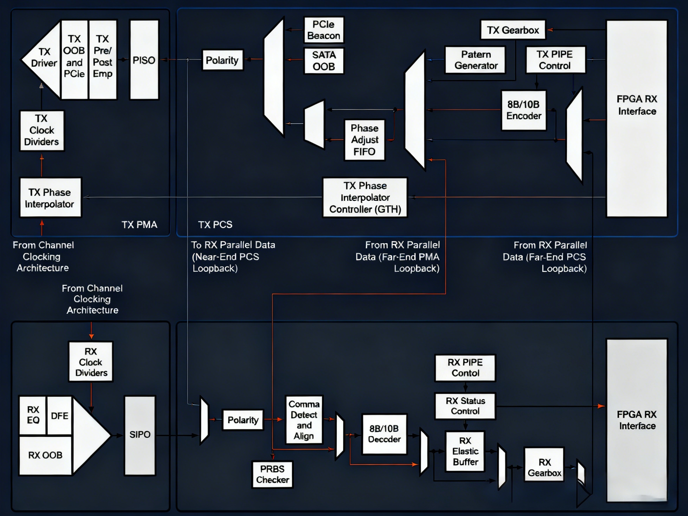
Functions of Each Physical Layer
a) The PCS layer handles data stream encoding/decoding. It is standard CMOS digital logic that can be implemented through logic synthesis for both software and hardware implementation.
b) The PMA layer, a mixed-signal CML/CMOS circuit, handles serialization/deserialization. Understanding this is key to distinguishing SerDes from parallel interfaces.
c) PMD layer: Responsible for serial signal communication.
5.2 Single-/Multi-lane
SerDes single-lane and multi-lane architectures represent two key approaches addressing differing performance requirements and cost considerations.
Simply put: Single-lane uses one pair of differential signals (TX+/TX-) for transmission and one pair (RX+/RX-) for reception. Its goal is to maximize the data rate per lane. Multi-lane bonds multiple single-lane units together to operate in parallel, achieving higher aggregate bandwidth.
(1) Single-Lane SerDes
Single-lane represents the most fundamental form of SerDes, focusing on continuously increasing transmission rates over a single differential pair.
Architecture
One transmitter (Serializer + TX Driver) -> One differential pair (Lane 0 TX+/-).
One receiver (RX Equalizer + Clock and Data Recovery + Deserializer) <- One differential pair (Lane 0 RX+/-).
Technical Features
The primary trajectory of technological advancement has been the continuous increase in single-lane baud rates. Starting from early generations of several Gbps, it has evolved to today's 112 Gbps and beyond. When NRZ (Non-Return-to-Zero) encoding encounters physical limitations, more efficient modulation schemes like PAM4 (Pulse Amplitude Modulation with four levels) are adopted. PAM4 transmits two bits per symbol cycle (00, 01, 10, 11), effectively doubling the data rate. To counteract high-speed losses and interference, highly complex equalization techniques are required, including FFE (Feedforward Equalization) at the transmitter and CTLE (Continuous-Time Linear Equalization) and DFE (Decision Feedback Equalization) at the receiver.
Advantages
Fewer chip pins, reduced PCB routing space, and potentially lower layer requirements. For applications requiring specific bandwidth, the total cost may be lower if a single channel suffices.
Disadvantages
Rate increases are constrained by physical laws (e.g., channel loss, noise), demanding extremely high standards for process technology, materials, and design.
(2) Multi-Channel SerDes (Multi-Lane)
When single-channel rate increases hit a bottleneck or ultra-high bandwidth is required, adopting a multi-channel parallel approach is the most direct and effective solution.
Architecture
Combines N identical single-lane SerDes physical layers (PHYs).
Logically, high-level data is split across these N channels for parallel transmission, then recombined at the receiver.
Examples: x4 (4 lanes), x8 (8 lanes), x16 (16 lanes) configurations.
Technical Features
Lane bonding is the core of multi-lane technology. Precise measurement and compensation of skew between all lanes must be ensured. Skew refers to the time difference when data propagates through lanes of varying lengths. The receiver requires a skew compensation buffer to align data from all lanes. Some protocols (e.g., PCIe) support Lane Reversal and Polarity Inversion, enhancing PCB routing flexibility. In cases of partial lane failure, specific systems can downgrade to operate in a reduced-lane mode (e.g., x8 to x4).
Advantages
Achieving ultra-high total bandwidth: Total bandwidth = Single-channel rate × Number of channels. This is currently the only viable approach to achieving Tbps-level bandwidth. For a given total bandwidth, increasing the number of channels reduces the required rate per channel, thereby lowering the design complexity and cost associated with signal integrity.
Disadvantages
Chips require more pins (more differential pairs), PCBs require routing more traces, occupying more space and potentially requiring additional layers. More SerDes PHYs and more complex PCBs typically translate to higher overall costs.
5.3 NRZ vs PAM4
(1) NRZ (PAM2)
Advantages include simplicity, high noise tolerance (sufficient eye height), and relatively low power consumption. A disadvantage is that the symbol rate (baud rate) equals the bit rate. Achieving higher data rates requires greater bandwidth, where channel loss increases sharply with frequency, becoming a bottleneck.
(2) PAM4
Advantages include doubling the data transfer rate at the same symbol rate compared to NRZ, effectively reducing channel bandwidth requirements. Disadvantages include extremely high SNR demands, three eye diagrams, and level spacing only one-third that of NRZ, making it highly sensitive to noise and interference. Higher power consumption necessitates more complex linear TX drivers and RX analog front ends (AFEs) to generate and detect multiple levels precisely. Higher BER: its native BER is worse than NRZ over the same physical channel.
5.4 LVDS/Camera/Automotive SerDes
(1) LVDS
Single-ended signals suffice for low-speed serial communication, while medium-to-high speeds necessitate differential signals—e.g., CAN bus employs medium-speed differential signaling. For higher data rates, multiple differential technologies exist. The table below lists the most common differential signal techniques and their key parameters.
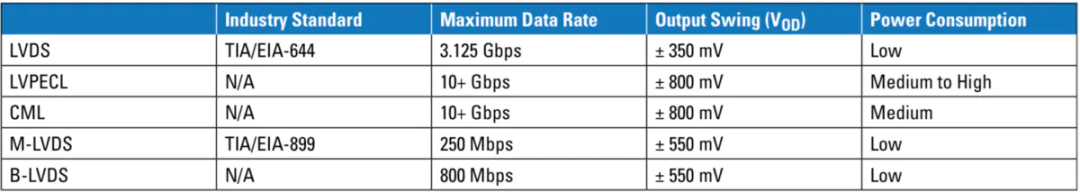
LVDS stands for Low-Voltage Differential Signaling. It features the lowest signal swing at 350mV, low power consumption, and a maximum data rate of 3.125Gbps.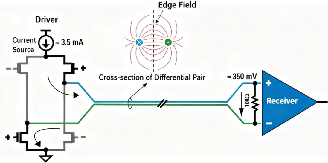
Overall, LVDS's advantages—including simple termination methods, low power consumption, and low noise—make it the preferred choice for applications ranging from tens of Mbps to 3 Gbps.
Additionally, as automotive applications demand increasingly higher communication speeds, high-speed technologies like LVPECL and CML are gaining traction. CML, in particular, offers comparable performance to LVPECL while featuring more straightforward implementation and integrated termination circuitry.
CML is a high-speed point-to-point interface with termination networks integrated into both the driver and receiver. It employs a passive pull-up circuit with a typical impedance of 50 ohms and utilizes an AC-coupled implementation to achieve data rates exceeding 10 Gbps.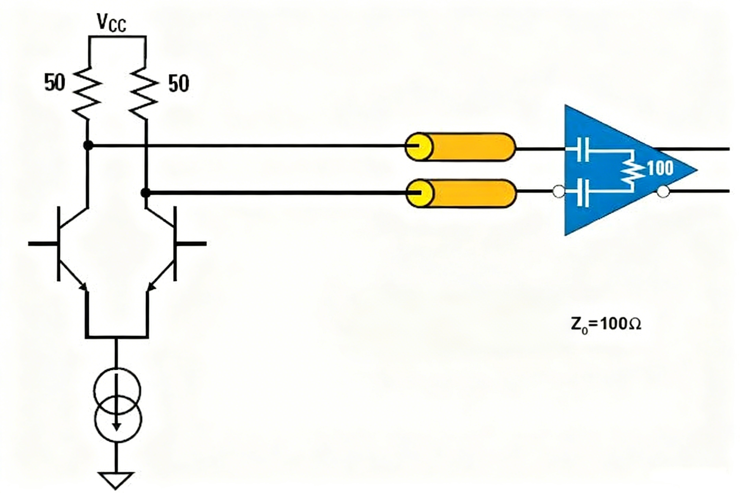
CML offers high data rates, but its increased swing also results in higher power consumption compared to LVDS.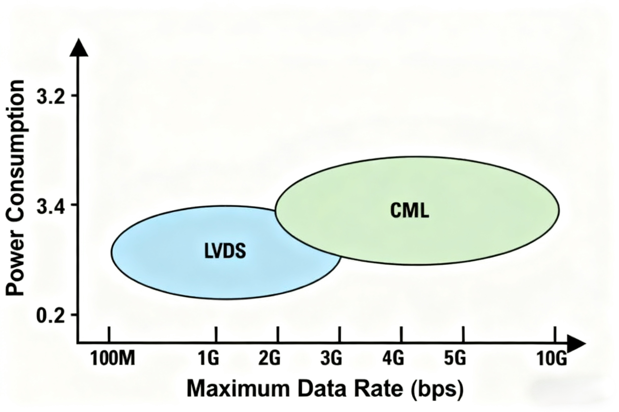
LVDS, CML, and LVPECL are all specifically designed for point-to-point signal transmission.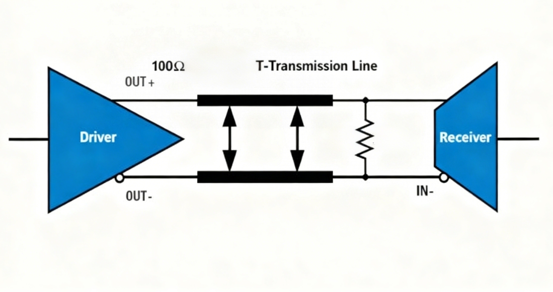
The other two variants, B-LVDS and M-LVDS, are optimized for multi-point structures based on LVDS, supporting multi-branch and multi-point transmission.
In summary, LVDS and CML are commonly used high-speed interfaces, with LVDS being the most widely adopted high-speed interface among differential signaling solutions!
(2) Automotive High-Speed SerDes
LVDS is a differential signal transmission method and one of the high-speed hardwired interfaces, while SerDes is a serialization and deserialization architecture that can be categorized into different protocol architectures.
Unifying hardware interfaces and protocol standards could yield a universal SerDes solution standard bus, much like how ISO standardized the CAN bus!
However, due to technical, market, and timing factors, public SerDes protocol standards have yet to gain widespread adoption. Current market solutions primarily rely on proprietary protocols from individual companies—meaning each company uses different protocols. These include FPD-LINK, GMSL, APIX, GVIF, and others. Among these, FPD-LINK and GMSL dominate 95% of the global market share, becoming representative SerDes solutions.
FPD-LINK, short for Flat Panel Display Link, is a high-speed digital video interface introduced by National Instruments. It connects the output of the graphics processing unit in laptops, tablets, flat-panel displays, or LCD TVs to the timing controller of the display panel. It was also the first LVDS standard to achieve large-scale bus implementation.
In automotive applications, FPD-LINK is commonly used in navigation systems, infotainment, cameras, and advanced driver assistance systems (ADAS). Given the automotive environment's stringent demands on electronics, current mainstream FPD-LINK II and III chips meet the AEC-Q100 automotive reliability standard.
GMSL is Maxim Integrated's automotive SerDes bus for high-performance cameras and HD video connectivity. GMSL supports daisy-chain connections for multiple camera modules.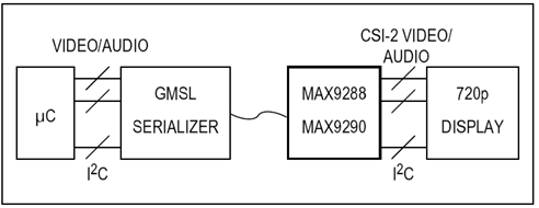
5.5 Redriver vs Retimer
PCI Express is a standard high-speed peripheral interface, a high-performance interconnect offering high bandwidth, scalability, and hot-plug capability. While data rates in PCIe have increased, the distances signals must traverse have not shortened. PCIe Gen5, released in 2019, achieves a single lane/channel rate of 32Gbps. In many cases, these distances are even longer.
To leverage higher data rates, PCIe links from Gen3 onward employ more efficient data encoding (8b/10b to 128b/130b) to improve data utilization. Lower-loss materials support Gen4 and Gen5 signals.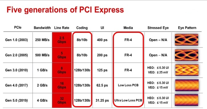
Even with lower-loss materials and advanced device-level equalization, the demand for in-channel PCIe signal conditioning continues to grow. PCIe introduced signal conditioning capabilities directly into the base specification for the first time in PCIe Gen4.
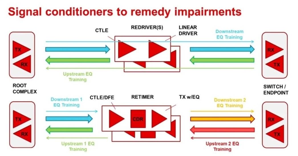
Signal conditioning functions used in PCIe systems fall into two categories: protocol-aware retimers and protocol-agnostic linear repeaters.
Retimers are relatively complex functions fully embedded within the system protocol. Linear repeaters, conversely, are completely protocol-agnostic. They employ analog equalization techniques solely to widen the eye opening, making the entire channel appear to the PCIe receiver with reduced attenuation.
The maximum channel loss in the PCIe standard has evolved from several dB in the first generation to over 35 dB in the upcoming fifth-generation specification.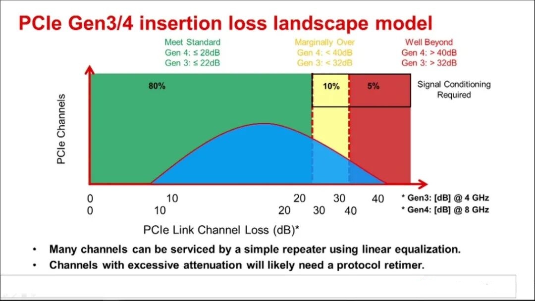
Despite employing multiple methods to reduce loss, some channels still experience attenuation exceeding PCIe specification limits. One approach to counteract increasing attenuation is using relatively simple linear repeaters or protocol-aware retimers.
A repeater or transceiver driver functions as an equalizer, employing continuous-time linear equalization (CTLE) to provide linear boost for high-frequency waveform components. This compensates for a portion of the channel's total loss.
Transceiver CTLE and linear driver functions can work together to reconstruct the analog transmit waveform characteristics and send them to the system receiver (RX). This purely analog approach enables direct communication between the system host and endpoint devices during single-link negotiation.
In contrast, the retimer strictly adheres to the PCI Express protocol. Utilizing the retimer to divide complex, non-compliant long PCIe channels into two segments creates a compliant upstream and downstream channel topology. The retimer directly participates in equalization negotiation for both upstream and downstream directions, allowing each to optimize its equalization settings independently. This effectively doubles the maximum link attenuation permitted by the standard.
If a bridge driver cannot correct excessive attenuation or the channel is overly complex, the retimer provides an ideal solution.
Another difference between retimers and transceiver drivers lies in device latency.
The protocol awareness and data retiming functions built into retimers introduce additional delay, reaching up to 64 nanoseconds in fourth-generation implementations. The linear approach of transceiver drivers significantly reduces solution delay to approximately 100 picoseconds.
In specific applications, using a transceiver with lower delay may be paramount. In others, enhancing retimer performance is the only way to achieve a stable, reliable solution.
Retimers and transceiver drivers represent two distinct approaches to solving the same problem.
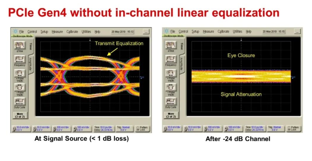
Here we observe a channel with 24dB attenuation and an 8GHz frequency. Due to the substantial channel loss, no open eye remains in the residual signal. Even with transmit equalization enabled, the intersymbol interference caused by attenuation still results in jitter large enough to completely close the open eye. The channel loss for this incoming signal approaches the limit for PCIe Gen4.
Therefore, even with the eye completely closed, the PCIe receiver is expected to correctly compensate for the attenuation and recover data from the incoming signal.
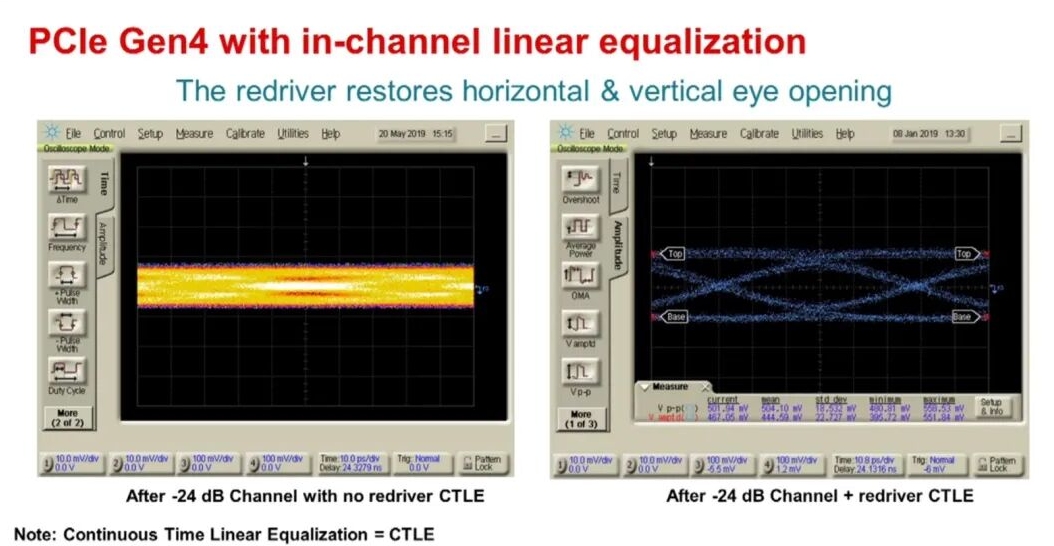
Here, we see how the added transceiver driver for the PCIe link helps compensate for channel attenuation. As mentioned earlier, the transceiver driver compensates for high-frequency losses in the transmission medium and restores both horizontal and vertical eye opening, as well as the received waveform.
Remember, the purpose of linear equalization is to shorten the effective channel length and reduce the loss imposed on the system's PCIe receiver. This pair of oscilloscope waveforms demonstrates linear equalization at 8GHz, which increases channel attenuation by approximately 14dB.
The system receiver does not perceive this increased attenuation because the linear equalization preserves the original waveform amplitude and waveform characteristics. Applying the same ±14dB equalization within a -40dB channel reduces the channel loss to approximately -26dB, meeting PCIe Gen4 specifications.
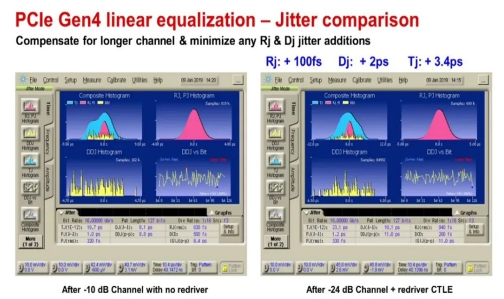
In this example, an oscilloscope is used to identify and measure both random and deterministic jitter components. Comparing jitter with and without the adapter driver demonstrates two key attributes of high-quality linear equalization.
First, we observe only a slight increase in the signal's random jitter. In this case, +100 femtoseconds resulted in a deplorable situation.
Second, the deterministic jitter in the signal is minimal.
In this case, this jitter is two picoseconds. With this analog performance, when channel attenuation increases by 14 dB, the total margin degradation is only 3.4 picoseconds. For fourth-generation signals, this value is merely 0.05 UI.
There is no need to worry about using linear equalization delay, as the typical delay of a linear equalization repeater is only 100 picoseconds. This is not significantly lower than the delay when the signal propagates along the transmission line itself.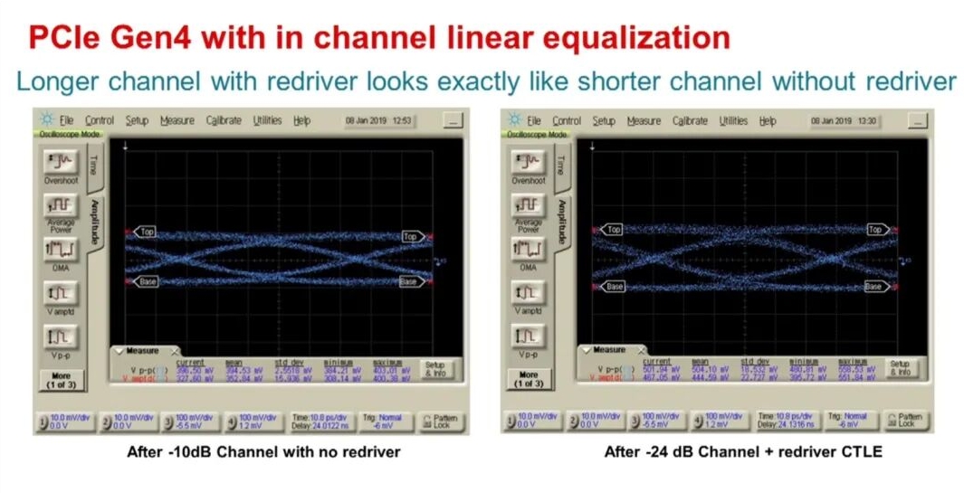
6.SerDes in FPGAs & SoCs
6.1 FPGA Use Cases
SERDES serves as a critical component in specific FPGA designs, enabling high-speed communication between various devices or systems. By converting parallel data to serial and vice versa, SERDES facilitates the rapid transmission of large data volumes while reducing power consumption and EMI emissions.
FPGAs leverage SERDES technology to transmit data through high-speed serial communication links operating at speeds reaching several gigabits per second. These links facilitate communication with external devices such as other FPGAs, CPUs, memory, or network interfaces.
Everyday Use Cases for SERDES in FPGAs
(1) High-Speed Data Transfer
SERDES technology is employed for high-speed data transfer between FPGAs or between FPGAs and other system components such as memory, processors, and network interfaces. This is typically utilized in data centers, telecommunications, and high-performance computing systems.
Lattice's Avant™ 16nm FinFET platform features 25 Gb/s SERDES to meet diverse application requirements, including high-speed data transmission.
(2) Optical Communication and Networking Applications
SERDES technology is a critical component for implementing many communication protocols, such as PCIe and Ethernet. PCIe is designed to meet growing bandwidth demands by enabling scalable point-to-point serial connections between chips via cables or expansion card connector slots. It also ensures software compatibility with traditional Peripheral Component Interconnect (PCI).
Lattice CertusPro™-NX FPGAs support 10G SERDES, enabling PCIe Gen 3 and 10G Ethernet up to 10G.
(3) Video and Audio Processing
FPGAs utilizing SERDES technology are also commonly employed in video and audio processing applications, managing high-speed data streams and performing tasks such as video decoding, encoding, and compression.
Lattice CrossLink™-NX FPGAs feature embedded MIPI D-PHY interfaces (CSI and DSI). This industry-standard protocol relies on SERDES technology.
(4) Industrial Automation and Robotics
Seamless communication between modules is enabled through industrial networking protocols.
FPGAs plays a role in three major industrial applications: real-time processing, advanced control, and electronic instrumentation.
The CertusPro-NX Versa Board helps designers evaluate designs for industrial markets and provides engineers with a prototyping and testing platform.
(5) Automotive Applications
Modern vehicles employ various sensors and cameras to support their ADAS capabilities. The data collected by these sensors and cameras requires preprocessing to remove noise and ensure proper formatting.
While some cameras and sensors adhere to MIPI standards, others utilize high-speed SERDES for extended-distance connectivity. Discover how Lattice FPGAs meet the demands of next-generation automotive applications requiring higher performance.
SERDES-Enhanced FPGAs
By combining high-speed serial data transceivers with programmable logic, SERDES-enhanced FPGAs deliver exceptional flexibility and architectural freedom. This empowers system designers to achieve application functionality and performance unmatched by other technologies. Additionally, FPGAs accelerate development cycles and offer programmability to adapt to evolving system standards. As a leader in low-power programmability, Lattice provides SERDES-enhanced FPGAs to help your designs reach their full potential.
6.2 Built-in vs Discrete
(1) As an Integrated IP Core
This is the most common and mainstream form of SerDes. It is not a standalone chip but rather an intellectual property (IP) module integrated into a larger chip (such as an SoC, FPGA, GPU, or CPU) during the design phase.
Analogy: This is like a compressor already installed inside a large appliance (e.g., a refrigerator). You don't buy the compressor separately when purchasing a fridge; it is one of the core components, specifically designed to serve the refrigerator's overall functionality.
Specific Description
Forms of existence: In ASICs or SoCs: Exists as complex macros or soft IP. For example, mobile processors (SoCs) integrate multiple MIPI D-PHY/C-PHY SerDes for connecting cameras and displays, and also incorporate PCIe SerDes for high-speed data exchange. In FPGAs: Pre-hardened as complex IP on silicon for optimal performance. Examples include GTH/GTY transceivers in Xilinx/AMD UltraScale+ FPGAs, LVDS SERDES in Intel FPGAs, or hardened IP for PCIe. Soft IP implementations exist but typically offer inferior performance.
Features
High Performance, Low Latency: Direct integration within the chip minimizes interconnect routing to other components, enabling extremely high speeds with minimal power consumption and latency.
High Bandwidth Density: Dozens or even hundreds of SerDes channels can be integrated onto a single chip (e.g., high-end switch chips).
Cost-optimized: For mass production, the integrated solution eliminates additional chip, PCB area, packaging, and pin costs, resulting in lower overall expenses.
Low Power Consumption: On-chip interconnect power consumption is significantly lower than that of PCB traces driving signals between chips.
Limited flexibility: Once manufactured, the SerDes type, data rate, and protocol support are fixed and cannot be upgraded.
Application Scenarios
Computing chips: PCIe and DDR controller interfaces in CPUs and GPUs.
Mobile Platforms: MIPI and USB interfaces in mobile SoCs.
Network chips: Ethernet (1G/10G/100G...) SerDes in switch and router chips.
Storage controllers: SATA, SAS controllers.
FPGA: Nearly all mid-to-high-end FPGAs integrate multiple high-speed SerDes hard cores for implementing various protocols.
(2) As a standalone chip (Standalone Chip / PHY)
In this form, SerDes functions as a standalone, single-purpose physical layer (PHY) chip. It typically serves as a bridging or expansion device, connecting chips lacking high-speed serial interfaces to high-speed serial links.
Analogy: This is like an external compressor. If your old refrigerator's compressor fails, or you want to upgrade the cooling capacity of a small freezer, you can attach one externally.
Specific Description
Form Factor: A standalone chip, typically connected to the host controller via parallel buses (e.g., PCIe, SGMII, XAUI) or serial buses. Its function is highly specialized: primarily handling serial-to-parallel/parallel-to-serial conversion and physical layer signal processing, while protocol handling remains the responsibility of the host chip.
Features
High Flexibility: Adds high-speed connectivity (e.g., 10 Gigabit Ethernet, PCIe) to legacy or low-cost host chips lacking native high-speed interfaces (e.g., microcontrollers, entry-level FPGAs).
Upgrading and Bridging: Commonly used for protocol conversion or interface expansion, such as interface cards/chips converting PCIe to SATA or USB.
Performance Overhead: Data must exit the main chip, traverse the PCB to the SerDes chip, and undergo processing, introducing additional latency, power consumption, and PCB design complexity.
Higher Cost: Requires additional chip expenses, PCB area, power supply, and thermal management considerations.
Design Complexity: Demands high PCB layout and routing standards with thorough consideration for high-speed signal integrity.
Application Scenarios
Interface Expansion Cards: Adds extra network ports (e.g., 10G NIC) to server motherboards, where the PHY chip functions as a standalone SerDes.
Protocol conversion bridge chips: Examples include DisplayPort-to-HDMI adapters, USB-to-SATA hard drive enclosure controllers, and PCIe-to-Ethernet chips.
Legacy System Upgrades: In industrial or embedded domains, adding high-speed serial communication capabilities to existing parallel bus-based systems.
Test and measurement equipment: Interface modules for instruments and meters, requiring flexibility and adaptability.
Summary and Comparison
|
Characteristics |
Integrated IP |
Standalone Chip |
|
Form Factor |
As a module within a larger chip |
A dedicated standalone chip |
|
Core Value |
Performance, power consumption, cost, integration |
Flexibility, bridging, and functional expansion |
|
Advantages |
High performance, low latency, low power consumption, high bandwidth density, low total cost |
Design flexibility, upgradability, cross-protocol bridging capability, independent of host chip functionality |
|
Disadvantages |
Low flexibility, cannot be modified once finalized |
Higher latency, greater power consumption, increased overall cost and PCB design complexity |
|
Typical Applications |
CPU, GPU, SoC, switch chips, high-end FPGAs |
Interface expansion cards, protocol converters, legacy system upgrades, test equipment |
6.3 Clocks & Jitter
The vast majority of SerDes protocols (e.g., PCIe, SATA, USB 3.0+, Ethernet) do not utilize dedicated clock lines. At extremely high frequencies (GHz range), it is challenging to ensure a dedicated clock line is perfectly equal in length to the data lines. Any minute-length discrepancy causes clock skew, leading to sampling errors. Adding clock lines necessitates more pins and PCB traces, increasing cost and design complexity.
Solution: Embedded Clock
The transmitter (TX) SerDes chip uses a local reference clock.
The serializer "encodes" clock information into the data stream when converting parallel data to a serial stream. This is achieved by ensuring the data stream contains sufficient level transitions (from 0 to 1 or from 1 to 0). For example, encoding schemes like 8b/10b, 64b/66b, or 128b/130b guarantee DC balance and transition density in the data.
At the receiver (RX) end, the core of the SerDes chip is a circuit called CDR (Clock Data Recovery). The CDR circuit functions like an exact phase-locked loop (PLL). It extracts the clock frequency and phase by monitoring the transition edges of the incoming data stream, thereby generating a clock that is perfectly synchronized with the incoming data. This clock is used for precise data sampling.
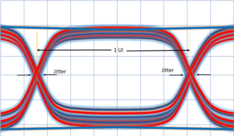
In high-speed digital signal transmission, jitter refers to the deviation of signal edges (rising or falling edges) from their ideal timing positions. It manifests as minute variations in signal period or phase, potentially causing data sampling errors and affecting system stability. Jitter is typically measured in picoseconds (ps) or unit intervals (UI), where 1 UI equals one bit period (e.g., 1 UI for a 10 Gbps signal equals 100 ps), as shown in the figure.
Jitter originates from various sources, such as:
Clock source instability (e.g., crystal oscillator phase noise)
Loss and reflection in transmission media (e.g., impedance mismatch in PCB traces or cables)
Crosstalk and noise (effects from adjacent signals or power supply noise)
Data-dependent jitter (DDJ) (e.g., intersymbol interference ISI).
Jitter is a critical timing error in high-speed digital signal transmission that directly impacts system stability, reliability, and performance, such as:
Causing data sampling errors: In high-speed serial communications (e.g., PCIe, USB, DDR, Ethernet), data must be correctly sampled within an extremely narrow time window (unit interval, UI). Excessive jitter may cause the receiver to sample incorrect levels (0→1 or 1→0), resulting in bit errors (BER). Exceeding the BER threshold prevents stable system operation.
Impacts clock recovery In SerDes (Serializer/Deserializer) systems, receivers rely on CDR (Clock Data Recovery) to extract the clock from the data stream. High-frequency jitter (especially RJ) may prevent CDR from locking onto the correct phase, causing link training failure. For instance, USB4 and Thunderbolt may throttle down or disconnect due to excessive jitter.
Reduced Signal Integrity Jitter narrows the horizontal width (eye width) and reduces the vertical height (eye height) of the eye diagram. A closed eye diagram indicates deteriorated signal quality, potentially preventing the receiver from correctly decoding data. Additionally, excessive jitter can render equalization algorithms ineffective, preventing signal recovery.
7. Design Flow & "How to Use SerDes"
SerDes design is a typical system-level engineering effort involving multiple stages including the chip, package, PCB, and connectors. Its core objective is to meet performance requirements at the target bit error rate (BER) with minimal cost and power consumption. This is achieved through rational allocation and coordinated design of Tx, Rx, and channel budgets under given channel conditions.
The entire design flow can be summarized as the following closed-loop process:
Requirement Definition → Budget Breakdown → Modeling & Simulation → Implementation (Layout & Materials) → Debugging & Verification → Compliance Certification
7.1 Requirements → Budget
This is the starting point for all designs, determining the direction and metrics for all subsequent work.
(1) Rate and Distance
Requirements: What data rate is required for the project (e.g., 16 Gbps)? How far must signals travel (on-chip, board-level, backplane, cable)?
Budget Impact: Rate and distance directly determine channel loss magnitude, serving as the core input for budget breakdown.
(2) BER Target
Requirement: What bit error rate can the system tolerate? Typically 10⁻¹² (PCIe, Ethernet) or more stringent 10⁻¹⁵ (Fibre Channel).
Budget Impact: The BER target directly determines the total jitter (TJ@BER) tolerance. Stricter BER requirements allow for lower permissible TJ.
(3) Insertion Loss/Return Loss and Jitter Budget (Tx/Channel/Rx Breakdown)
This process allocates the system's total performance "pie" across three components.
Channel Insertion Loss: @Nyquist frequency (i.e., 1/2 baud rate). For example, the Nyquist frequency for a 32Gbps NRZ signal is 16GHz. Empirical rules (e.g., PCIe specifications) define explicit limits for total channel insertion loss (e.g., -36dB @16GHz for PCIe 5.0).
Channel Return Loss: Reflections exacerbate ISI, so return loss must also be specified (e.g., < -10 dB).
Jitter Budget
Tx DJ/RJ: Deterministic jitter and random jitter generated by the transmitter chip.
Rx DJ/RJ: Jitter introduced by receiver clock recovery circuits, etc.
Channel DJ: Primarily jitter introduced by channel ISI.
Power and Complexity: Budget allocation involves trade-offs between performance, power consumption, and cost. Allocating more budget to Tx (stronger pre-emphasis) increases Tx power consumption; allocating more to Rx (stronger equalization like multi-tap DFE) increases Rx complexity/area/power consumption; allocating more to Channel (better PCB materials, shorter distance) increases cost.
7.2 Modeling
Pre-production simulation through modeling is critical before committing to expensive manufacturing and testing.
(1) S-parameters (Channel)
What it is: A model describing the frequency-domain characteristics of a channel, including insertion loss (S21), return loss (S11/S22), and crosstalk (S31, etc.).
How to Use: Obtain S-parameter models (Touchstone format, e.g., .s4p) from PCB, connector, and cable manufacturers. Cascade these S-parameters in simulation software (e.g., ANSYS HFSS, Keysight ADS, Cadence PowerSI) to build a complete channel model from the TX chip pad to the RX chip pad.
(2) IBIS-AMI (Transceiver)
What it is: An industry-standard behavioral-level model for SerDes.
IBIS: Describes the electrical characteristics of the Tx/Rx analog front end (e.g., IV/VT curves, package models).
AMI: Describes the algorithmic portion (e.g., Tx FFE, Rx CTLE/DFE, CDR), provided as compiled (.dll/.so) files.
How to use: Connect the IBIS-AMI model provided by the chip vendor with the channel's S-parameter model in a simulation platform (e.g., ADS) to perform statistical analysis (StatEye) or time-domain bit-by-bit simulation.
(3) PRBS/Eye/BER Target Setting
PRBS: Most commonly used test patterns (e.g., PRBS7, PRBS31) to simulate random data and excite worst-case ISI conditions.
Simulation Objective: Adjust equalization parameters (tap weights, CTLE gain) via the AMI model to observe whether the generated eye diagram opens and whether the BER level on the bathtub curve maintains sufficient eye height/eye margin at the target BER.
7.3 Equalization Plan
One core task of simulation is to formulate and validate equalization strategies.
(1) TX FFE Tap Planning
FFE is a finite impulse response (FIR) filter with pre-distortion. Commonly used are 3-tap or 5-tap configurations.
Strategy: Scan the weight combinations of Pre-cursor and Post-cursor taps through simulation to identify the optimal settings that most effectively compensate for channel loss and provide the cleanest signal to the receiver.
(2) RX CTLE Curve/DFE Tap
CTLE: Provides selectable frequency response curves (Peaking gain). Simulate to choose the curve that best cancels channel loss, preparing the DFE.
DFE: Nonlinear equalizer that effectively eliminates ISI. Simulation targets determining the number of taps required (e.g., 5-tap DFE) and their weights to ensure correct sampling even under severe conditions.
(3) Training and Adaptive Strategy
Requirement: Many protocols (e.g., PCIe) support automatic negotiation between transmitter and receiver during the power-up link training phase to adjust to optimal equalizer settings.
Strategy: Verify in simulation whether the adaptive algorithm converges near the expected optimal settings.
7.4 Layout & Materials
Simulation results will guide physical implementation.
Routing Geometry: Determine trace width and thickness based on simulation-defined loss targets to control impedance (typically 100Ω differential).
Materials: Select PCB laminate dielectric constant (Dk) and loss tangent (Df). Low-Df materials (e.g., Megtron 6, FR408HR) are commonly used in high-speed designs to minimize loss.
Surface Roughness: Copper surface roughness significantly increases high-frequency loss; smooth copper (e.g., HVLP/RTF) must be specified.
Via/Backdrill: Via stubs introduce severe resonance and reflections; backdrill technology must be used to eliminate unwanted stubs.
Connector and Cable Selection: Select connectors and cables that meet applicable specifications (e.g., SFP+, QSFP-DD) and achieve required S-parameter performance based on data rate and mechanical requirements.
7.5 Bring-up & Tuning
After hardware delivery, validate and fine-tune the design through actual testing.
PRBS Generation/Bit Error Counting: Use an oscilloscope or Bit Error Rate Tester (BERT) to have the Tx transmit PRBS patterns while the Rx performs error detection. This is the gold standard for verifying the link's fundamentals.
Eye Diagram/Bathtub Curve Observation: Capture signals using a high-speed oscilloscope (with PLL clock recovery and eye diagram software) to assess signal quality and compare with prior simulation results visually.
Frequency Sweep and Tap Scan
Sweep: Measure the S-parameters of the final PCB using a vector network analyzer (VNA) and compare them with the simulation model.
Tap Scanning: If link performance falls short of expectations, manually fine-tune the Tap weights of the Tx FFE or the Rx CTLE gain on the oscilloscope. Observe improvements in the eye diagram to identify the optimal solution.
7.6 Compliance
The final product must pass industry-standard compliance testing to ensure interoperability with other devices.
(1) Compliance Test Path
Use specified test fixtures (Compliance Board) and test equipment (e.g., high-speed oscilloscopes, BERT).
Rigorously execute the full suite of tests according to specifications published by standards organizations (PCI-SIG, IEEE, OIF), including Tx tests (eye diagram, jitter, equalization), Rx tests (tolerance testing), and link tests.
(2) Common Failure Modes
Tx: Excessive jitter, insufficient eye height/width, mismatched equalization settings.
Rx: Poor tolerance capability, bit errors under stress testing.
Channel: Resonance points (caused by via stubs or connectors), excessive return loss, and high crosstalk.
8. Applications & Scenarios
8.1 Data Center & HPC
Over the past six years, Ethernet speeds have escalated from 25G/50G to today's 400G, with 800G anticipated soon. As an indispensable component of hyperscale data centers, switch-supported bandwidth has surged from 12.8 terabits per second (Tb/s) to 25.6 Tb/s today, projected to reach 51.2 Tb/s within the next few years. As switch speeds advance to 51.2 Tb/s, 512 SerDes channels will be required, each operating at 100 Gb/s and comprising a combination of Very Short Range (VSR), Medium Range (MR), and Long Range (LR) SerDes.
Therefore, to meet system requirements, 112G SerDes must deliver optimized performance across all three interfaces: VSR, MR, and LR. As shown in the figure, hyperscale data centers continue to evolve to accommodate increasing Ethernet speeds, switch bandwidth, and evolving module types.
Within hyperscale data centers, SerDes face exceptionally demanding operational conditions. Merely meeting Interference Tolerance (ITOL) and Jitter Tolerance (JTOL) requirements is insufficient; stable performance must be maintained under multiple challenges, such as significant channel insertion loss, extreme temperature cycling, and diverse packaging types.
A 112G SerDes PHY architecture combining analog and digital modules optimally delivers peak performance, minimal power consumption, and the smallest footprint. For instance, the analog module assists the digital module with signal pre-emphasis, reducing DSP load, significantly lowering power consumption, and ensuring stable bit error rate (BER) performance. Similarly, the digital module helps the analog module compensate for linearity and other analog impairments caused by process, voltage, and temperature variations.
The 112G Ethernet PHY IP, fabricated in a 5nm FinFET process, incorporates an ADC and DSP architecture with power tuning technology that substantially reduces power consumption in low-loss channels. Through optimized PHY layout, it can be stacked and placed on all four edges of the die, maximizing overall chip bandwidth. Additionally, its unique architecture supports independent data rates per channel, enabling maximum flexibility. Recently, silicon verification of the 5nm DesignWare® 112G Ethernet PHY IP demonstrated zero BER with backward error correction in channels exceeding 40dB, while delivering power efficiency below five pJ/bit.
Beyond power, performance, and area efficiency, the 112G SerDes IP features comprehensive core functionality, including adaptive tuning and temperature tracking to further optimize real-world performance. It also achieves optimal adaptation between VSR and LR modes without external intervention, delivering exceptional performance.
Adaptive tuning capability: Achieves optimal adaptation between VSR and LR without external intervention, delivering outstanding performance.
Multiple rounds of tuning can be performed to achieve an optimized configuration.
Continuous Timeline Linear Equalization (CTLE) with boost amplifier/suppressor: The dynamic range of CTLE-boosted equalization is a critical consideration for operating across channel loss characteristics. For CTLE, operating without boost in low-loss channels is equally challenging as lacking boost in high-loss conditions. The 112G SerDes IP implements CTLE with additional boost amplifier/suppressor circuitry, expanding the dynamic range. This approach benefits by increasing the boost for long channels while reducing unnecessary boost for short channels, enabling accurate VSR-to-LR operation.
Achieving sampling point optimization: By adjusting clock sampling, the digital module of 112G SerDes IP can fine-tune performance across a wide channel range. The clock path sampling point can be adjusted relative to the data path sampling point, significantly improving performance from VSR to LR operation. Furthermore, the analog module can adjust ADC resolution by disabling unnecessary additional comparisons in low-resolution mode. This provides optimal power savings and channel distance;
Flexible Performance Knobs: For short-distance, low-loss channels, power consumption can be further reduced by disabling floating front-end equalization (FFE) taps, using fewer ADC conversions, and decreasing analog front-end (AFE) bias current and bandwidth;
Temperature Tracking: Ensures robust performance across PVT variations
It is well known that analog performance varies with temperature. For applications requiring operation over a wide temperature range, high-speed serial links can operate continuously without requiring re-initialization or re-adaptation. This capability is primarily achieved through the link receiver's continuous adaptive equalization, which compensates for channel parameter variations caused by temperature changes.
Two key features ensure optimal 112G performance across temperature variations
Temperature-Aware Continuous Calibration and Adaptation (CCA) ensures adaptive adjustments occur only when temperature changes, preventing channel performance degradation through optimized calibration and adaptive algorithms with intelligent implementation. Internal temperature sensors for die-level temperature measurement trigger specific adaptations, such as CTLE, only when specific temperature changes occur. Adaptive functions (e.g., receiver FFE, DFE) are periodically enabled to track any changes occurring in between.
Accurate positive/negative full-range temperature tracking: As shown in the figure, by monitoring and tracking temperatures across the entire range, the PHY can accept power supply at any intermediate temperature while maintaining high-level operation during heating or cooling cycles from -40°C to 125°C.
8.2 5G/Fronthaul & Telecom
(1) Optical Transport Network (OTN) & Core Routers/Switches
This is the most classic application domain for SerDes.
Applications: Interconnections between line cards and switching matrices in core routers and switches, as well as interfaces between these devices and optical modules.
How it works:
The network processor processes packets entering the line card.
SerDes chips (typically part of an ASIC or FPGA) convert the processed parallel data into high-speed serial data streams.
This serial data stream travels via PCB traces to optical modules (e.g., QS-DD, OSFP, CFP2).
Drivers and modulators within the optical module convert the electrical signal into an optical signal for long-distance transmission over fiber.
At the receiving end, the reverse process occurs.
Standards and Rates:
OTN: The foundational protocol for implementing telecommunications transport networks. SerDes serves as the physical layer implementation for OTN interfaces (e.g., OTU4).
Ethernet: High-speed Ethernet interfaces (e.g., 100GbE, 400GbE) are entirely built upon SerDes. For instance, 400GbE typically employs SerDes channels configured as 8x50G PAM4 or 4x100G PAM4.
OIF CEI: Standards defined by the Optical Interconnect Forum, such as CEI-56G and CEI-112G, specify the electrical characteristics of SerDes at ultra-high speeds. These form the foundation for the current 400G and future 800G optical module interfaces.
(2) Radio Access Network (RAN) - 4G/5G Base Stations
5G networks impose unprecedented demands for high bandwidth and low latency on fronthaul and backhaul.
eCPRI/CPRI Interface:
In traditional 4G and 5G distributed base stations, the radio unit (AAU/RRU) and baseband unit (BBU) are connected via CPRI or eCPRI protocols.
To meet 5G demands, eCPRI employs packet-based transmission, significantly reducing bandwidth requirements while still necessitating high-speed SerDes for data transmission over fiber.
SerDes technology is employed within AAU/RRU and BBU equipment, as well as in the optical modules connecting them.
5G Cloud-based Radio Access Network (C-RAN):
Under the C-RAN architecture, BBUs are centralized and cloud-based, operating at greater distances from AAUs. This places extremely high demands on the optical fiber network connecting AAUs to centralized BBUs, necessitating extensive use of optical transmission equipment based on high-speed SerDes.
(3) Data Center Interconnect (DCI)
High-speed interconnections between large telecom carrier data centers are essential, making DCI a critical component of telecommunications services.
Applications: DCI equipment employs technologies similar to core routers but prioritizes cost-effectiveness and density. They extensively utilize SerDes-based pluggable optical modules (e.g., 400G-ZR) to enable fiber-based interconnections between data centers.
(4) Network Function Virtualization (NFV) and Software-Defined Networking (SDN)
Telecom networks are evolving toward cloudification and virtualization. Hardware platforms supporting NFV and SDN (such as generic white-box switches/servers) rely on high-speed SerDes to enable rapid data exchange between virtual network functions (VNFs) and with the control plane.
8.3 Automotive
The automotive sector's adoption of SerDes technology to address communication link challenges is an inevitable choice in response to the surge in in-vehicle electronic devices and data transmission demands driven by intelligent and connected vehicle trends.
Key SerDes application scenarios in automotive include:
Intelligent Driving Systems: Cameras, lidars, and various sensors in autonomous driving and Advanced Driver Assistance Systems (ADAS) utilize SerDes for data transmission and communication with processors, meeting high-bandwidth and low-latency requirements. For instance, an 8-megapixel camera generates 5.75 Gbps of data per second, while Level 4 autonomous driving requires processing raw video streams from over 12 cameras. A traditional Mbps-level CAN bus cannot handle this load, necessitating SerDes adoption.
Smart Cockpit Systems: Devices including instrument clusters, infotainment screens, head-up displays, and streaming rearview mirrors transmit high-quality audio/video signals via SerDes to meet high-bandwidth and low-latency requirements. The three-screen cockpit (center console + instrument cluster + HUD) demands over 50 Gbps total bandwidth, far exceeding the capabilities of traditional LVDS (max 3 Gbps) and Ethernet (1 Gbps). Only SerDes solutions can handle this massive data flow.
In-vehicle Communication Systems: SerDes integrates with traditional protocols like CAN and LIN to achieve higher data transmission efficiency, supporting V2V (vehicle-to-vehicle) and V2I (vehicle-to-infrastructure) communications. SerDes' clock recovery technology (CDR) controls end-to-end latency at the nanosecond level, meeting the real-time requirements for autonomous driving decision-making.
Current Application Status
In automotive electronics, SerDes chips typically exist as a serializer + deserializer chipset, requiring strict protocol and speed matching. Due to protocol compatibility constraints, serializers and deserializers must be selected from the same brand and used in pairs.
ADAS Camera Transmission: Each camera requires one serializer chip. Deserializer chips typically support multiple channels (e.g., 4-in-1), with an average of one deserializer chip shared among every four cameras.
Smart Cockpit Displays: Each display requires an independent chipset pair, e.g., one set each for the center console screen, instrument cluster, and HUD.
Per-vehicle usage: L2/L3 autonomous vehicles require 8-16 serializer chips and 2-4 deserializer chips; premium models exceed 20 chips. Data rates: Current mainstream is 6-8Gbps, with future upgrades to 12.8Gbps (HSMT) and 24Gbps (PAM4 modulation), demanding higher integration in chipset designs.
8.4 Industrial & Vision
In machine vision, SerDes applications primarily manifest in interfaces between camera sensors and processors, as well as transmission protocols between cameras and host systems.
Inside modern high-end industrial cameras, image sensors (e.g., CMOS) generate extremely high output data rates (billions of pixels per second). Directly using parallel lines within the camera to transmit sensor data to the processing chip causes severe noise, synchronization, and power consumption issues.
Application: Camera chip designers integrate a miniature SerDes transmitter (Tx) next to the sensor and a receiver (Rx) on the image processing chip (or FPGA) side.
Advantages
Reduced internal wiring: Decreases dozens of parallel data lines to just a few differential pairs.
Reduce noise and power consumption: Fewer traces mean lower capacitive loading and cross-interference.
Enhanced integration: Enables more compact and reliable camera designs.
Common Standards: MIPI Alliance's C-PHY and D-PHY (commonly used in mobile and embedded cameras) and the higher-speed MIPI A-PHY (automotive/industrial grade) are essentially variants of SerDes technology.
9. Component Selection & BOM Guidance
9.1Retimer vs Redriver
|
Characteristics |
Redriver |
Retimer |
|
How It Works |
Analog amplifier. Provides gain (amplifies the signal) and configurable equalization (e.g., de-emphasis), but also amplifies noise and jitter. |
Mixed-signal device. Incorporates CDR (Clock Data Recovery) and retimer. It fully reconstructs the digital signal (1/0) before transmitting it with clean jitter characteristics. |
|
Core Functions |
Equalization (EQ), Amplification |
CDR, Equalization (EQ), Signal Reconstruction |
|
Jitter Handling |
No effect. It pass-throughs or even amplifies input signal jitter. |
Effectively Eliminated. Significantly reduces output jitter by retransmitting data using a new clock. |
|
Delay |
Extremely low (typically < 1 ns), purely analog path. |
Higher (typically 10-20 ns), requires digital processing time. |
|
Power consumption |
Low |
High (includes both analog and digital circuits) |
|
Cost |
Low |
High |
|
Applicable Scenarios |
Clean channels where insertion loss is the primary concern, but jitter is minimal. Examples: |
"Dirty" channels exhibit both significant insertion loss and jitter caused by reflections and crosstalk. Examples include: |
Selection Criteria
First, perform channel simulation. If simulation shows the eye diagram is closed but clean (low jitter), select a Redriver.
If simulation shows the eye diagram is closed but blurred (high jitter), or if actual measurements reveal excessively high BER, a Retimer must be used.
9.2 Refclk & Jitter Cleaner
(1) Reference Clock (Crystal Oscillator - XO)
Key Selection Parameters
Frequency: Must meet SerDes chip requirements (e.g., 156.25 MHz, 100 MHz, 125 MHz).
LVDS and HCSL are the most common differential output types for high-speed SerDes, offering strong noise immunity.
Phase Noise: This is the most critical metric. Must meet SerDes chip manual requirements at specified frequency offset points (e.g., 10 Hz, 100 Hz, 1 kHz, 10 kHz, 100 kHz, 1 MHz, 10 MHz). Lower phase noise directly translates to lower RJ.
Total Jitter: Typically requires less than 100 fs RMS over an integrated bandwidth of 12 kHz to 20 MHz.
Stability: For applications sensitive to temperature variations, consider ±25 ppm or tighter stability specifications.
(2) Jitter Cleaner / Clock Conditioner
When required?
When the system reference clock quality is poor.
When multiple clean clocks at different frequencies need to be generated from a single input clock to supply multiple SerDes devices.
When isolating downstream clock jitter from upstream clock sources.
Key Selection Parameters
Input/Output Frequency: Supports all required frequencies.
Output phase noise: Its performance determines the level of "cleanliness" it can provide.
Loop bandwidth: Adjustable bandwidth allows designers to filter out jitter outside the bandwidth (e.g., jitter from upstream sources).
Integrated VCXO: Typically incorporates an internal voltage-controlled crystal oscillator, whose quality defines the performance ceiling.
BOM Considerations: Reference clocks and jitter cleaners vary significantly in cost and quality; allocation must be precise based on the system's total jitter budget.
9.3 Connectors & Cables
(1) Key Selection Parameters
Protocol Compatibility: Must explicitly support required protocols and data rates (e.g., PCIe 4.0, SAS 4.0, 400GAUI-4).
S-parameter performance
Insertion Loss: Ensure loss at the Nyquist frequency remains within the equalization capability of the SerDes chip. For example, PCIe 5.0 requires total channel insertion loss @ 16 GHz <-36 dB.
Return Loss: Measures impedance matching quality; lower values are better (e.g., <- -10 dB). Poor return loss causes reflections, increasing jitter.
Crosstalk: Particularly Near-End Crosstalk (NEXT) and Far-End Crosstalk (FEXT).
Insertion Loss Window: This is a system-level concept. You must simulate the cascaded S-parameters of connectors/cables with PCB traces to ensure the total channel response falls within the equalization capability of the SerDes chip (or Retimer).
Common Types
Board-to-board connectors: High-speed series available from manufacturers like Samtec, Molex, and Amphenol. Focus on pin density, height, and S-parameter models.
Panel connectors: SFP+/SFP28 (10/25G), QSFP28/QSFP-DD/OSFP (100/400/800G). Select reputable brands (e.g., Amphenol, Molex, TE) to ensure consistency.
Cables
DAC: Direct Attach Cable, a passive copper cable that is low-cost and low-power-consuming, used for ultra-short-distance in-rack interconnects.
AEC: Active cable with built-in retimer or redriver, extending transmission distance.
Fiber Optic Cables: Used for long-distance transmission, requiring matching optical modules.
BOM Key Points: Never select components based solely on manufacturers' "supports XXX speed" claims. Always request and perform channel simulation using their 3D/2D S-parameter models.
9.4 Protection & EMC
(1) ESD Protection Components
Location: Positioned after the connector, at the point where signal lines enter the board.
Key Selection Criteria
Capacitance: Must be extremely low (typically <0.5 pF, even <0.2 pF) to avoid severe signal integrity degradation for high-speed signals.
Response time: <1 ns.
Standards: Must meet IEC 61000-4-2 Level 4 (±8kV contact, ±15kV air) or higher.
(2) Common Mode Choke (CMC)
Function: Suppresses common-mode noise (the primary source of EMI radiation) without affecting differential signals.
Key Selection Criteria
Differential Insertion Loss: Must be sufficiently low to avoid significant signal degradation.
Common-Mode Rejection: High rejection ratio within target frequency range (e.g., FCC/CE certified radiation bands).
Rated Current: Must meet power requirements.
(3) EMI Design (Implied BOM Costs)
Shielding Covers: Used to shield high-speed noise sources such as ASICs and SerDes chips.
Shielding Tape/Spring Foil: Used for gap shielding at interfaces and chassis.
PCB Laminate: Utilizes complete ground and power planes to provide tight return paths for high-speed signals—the most effective and cost-efficient method for EMI control.
BOM Key Points: ESD and CMC selection must be based on simulation using their S-parameter models to ensure noise suppression without closing the eye diagram. EMI-related materials are essential investments to ensure first-time certification success and avoid costly post-production modifications.
10. From Prototype to Mass Production
With the advancement of information and communication technology, demands for data transmission speed and efficiency continue to rise. Traditional parallel interfaces have reached a bottleneck in speed, making faster serial interfaces the prevailing technological trend. Consequently, SerDes technology—initially developed for fiber optic communications—has become the mainstream solution for high-speed serial interfaces.
SerDes automated testing has been constrained by limitations in test system transmission rates and hardware design, causing SerDes testing to lag significantly behind SerDes chip development. After years of R&D and accumulating high-speed I/O testing expertise, Advantest has developed a comprehensive test solution (Nautilus UDI) based on the 93000 platform, supporting rates up to 32.8 Gbps. This solution fills the gap in automated testing for high-speed I/O SerDes operating at 16G-32.8 Gbps. As shown in the figure, the 93000 platform provides SerDes test solutions supporting multiple transmission rates up to 9 Gbps, 16 Gbps, and 32.8 Gbps. 
Figure: 93000 0-32G Data Rate Test Solutions
SerDes is an abbreviation for Serializer/Deserializer. It is a mainstream Time Division Multiplexing (TDM), Point-to-Point (P2P) serial communication technology. Specifically, multiple low-speed parallel signals at the transmitter are converted into high-speed serial signals. These signals traverse the transmission medium (optical fiber or copper wire) and are reconverted into low-speed parallel signals at the receiver. Standard consumer electronics interfaces like PCIe and SATA exemplify SerDes technology applications.
SerDes primarily consists of a PLL-based clock module, control module, transmitter, and receiver. To address testing challenges and reduce costs, modern SerDes designs incorporate additional modules such as a pseudorandom bit sequence (PRBS) generator, PRBS verifier, and loop path to assist in testing.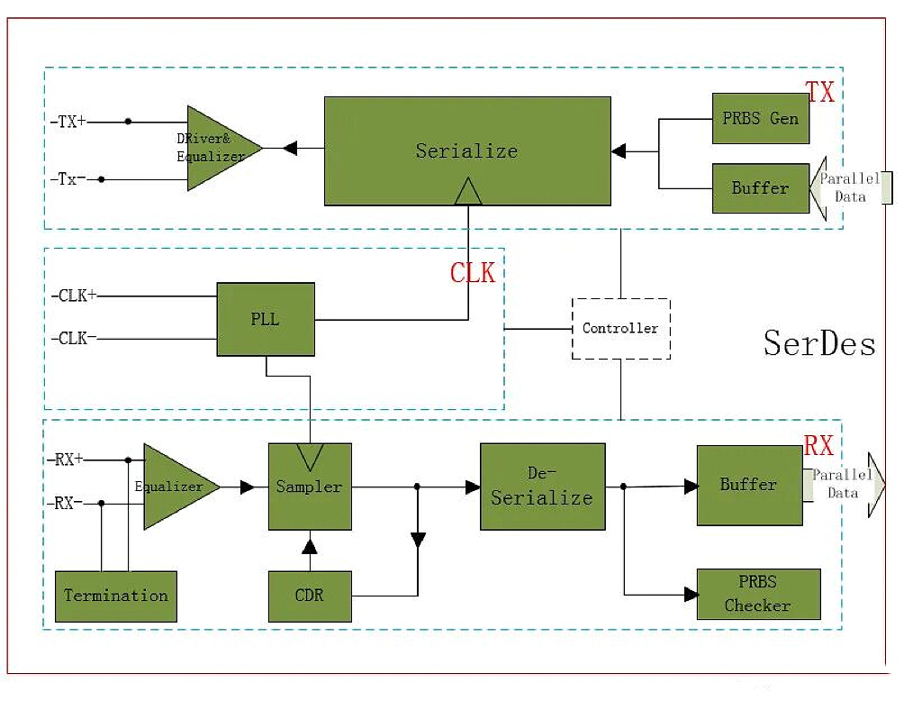
Figure: SerDes Architecture
10.1 SerDes Testing
SerDes testing primarily encompasses BIST (Built-in Self-Test) and high-speed I/O testing. BIST testing relies mainly on internal chip test modules to verify functional integrity. Its key advantages include high testing efficiency, low cost, and minimal hardware fabrication requirements (e.g., load boards). However, it cannot evaluate chip characteristics, offers relatively low test coverage, and lacks failure localization capabilities. High-speed I/O testing, conversely, can address nearly all SerDes testing needs with high coverage, but demands significant hardware fabrication resources and incurs higher testing costs.
SerDes high-speed I/O testing can be divided into two major categories based on test modules: receiver testing and transmitter testing. Key receiver performance metrics include: sensitivity testing, jitter tolerance testing, skew testing, and impedance testing. Transmitter performance metrics primarily include: output amplitude testing, eye height, eye width testing, rise/fall time testing, jitter testing (TJ, RJ/DJ), eye diagram testing, common-mode voltage testing, skew testing, impedance testing, etc.
10.2 Nautilus UDI Solution
The Nautilus UDI (hereafter referred to as UDI) solution is illustrated in the figure. The 93000 sends four 8 Gbps signals to the UDI, which internally multiplexes them into a single 32 Gbps signal for transmission to the chip. This combines with the chip's internal pseudorandom code verifier to perform receiver testing. The chip's internal transmitter sends a 32 Gbps signal, which is demultiplexed into four 8 Gbps signals by the DEMUX. These signals are then sampled, tested, and analyzed by the 93000, enabling transmitter testing. Leveraging the chip's parallel loopback model, we typically use loopback eye diagram testing in actual mass production to cover both receiver and transmitter functions. UDI supports test rates from 16 Gbps to 32.8 Gbps (with future scalability up to 64 Gbps), capable of testing up to 16 receiver and transmitter pairs simultaneously. 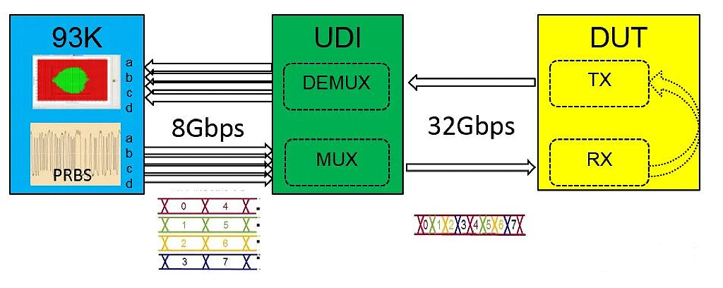
Figure: UDI Test Solution Model
(1) Nautilus UDI Operating Principle
The UDI primarily consists of two circuit sections: MUX and DEMUX. The MUX incorporates a 4:1 multiplexer (as shown in the figure).
The first-stage 2:1 multiplexer is controlled by the RX_CLK (4 GHz) x2 frequency-doubled clock to synthesize AC and BD signals.
After passing through a second-stage 2:1 multiplexer controlled by the X4 frequency-doubled clock, the signals are converted into ABCD. An output stage featuring an amplifier with adjustable gain (0–1200 mV) and a 10 dB attenuator provides an output range of 0–260 mV, meeting receiver sensitivity testing requirements for both functionality and precision.
Beyond triggering the multiplexer, the RX_CLK signal incorporates jitter injection to introduce signal jitter at the output, thereby testing receiver tolerance. The DEMUX structure approximates that of the MUX, incorporating a built-in 1:4 demultiplexer.
A passive equalizer is added before the DEMUX to flatten signals distorted by path insertion loss, thereby reducing inter-symbol interference caused by transmission paths. 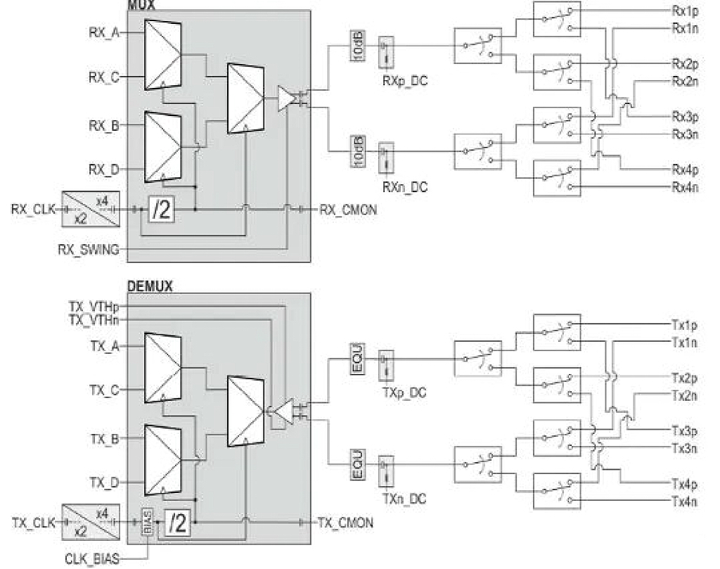
Figure: MUX and DEMUX Structures
(2) Chip Input Clock
SerDes imposes stringent requirements on reference clocks. Input clock RJ is mixed into the SerDes, preventing accurate measurement of the chip's true jitter. As shown in the figure, using a reference clock with RJ=1ps (SerDes requires RJ<400fs) resulted in excessive eye diagram scatter, compromising test stability. To address this, we selected a standardized Jitter Attenuator Module (JAM). Programmable control via the 93000 enabled noise reduction for different clock frequencies. After passing through the JAM, the reference clock RJ was reduced to below 300fs. The scanned eye diagram exhibited no scatter points, ensuring stable mass production testing.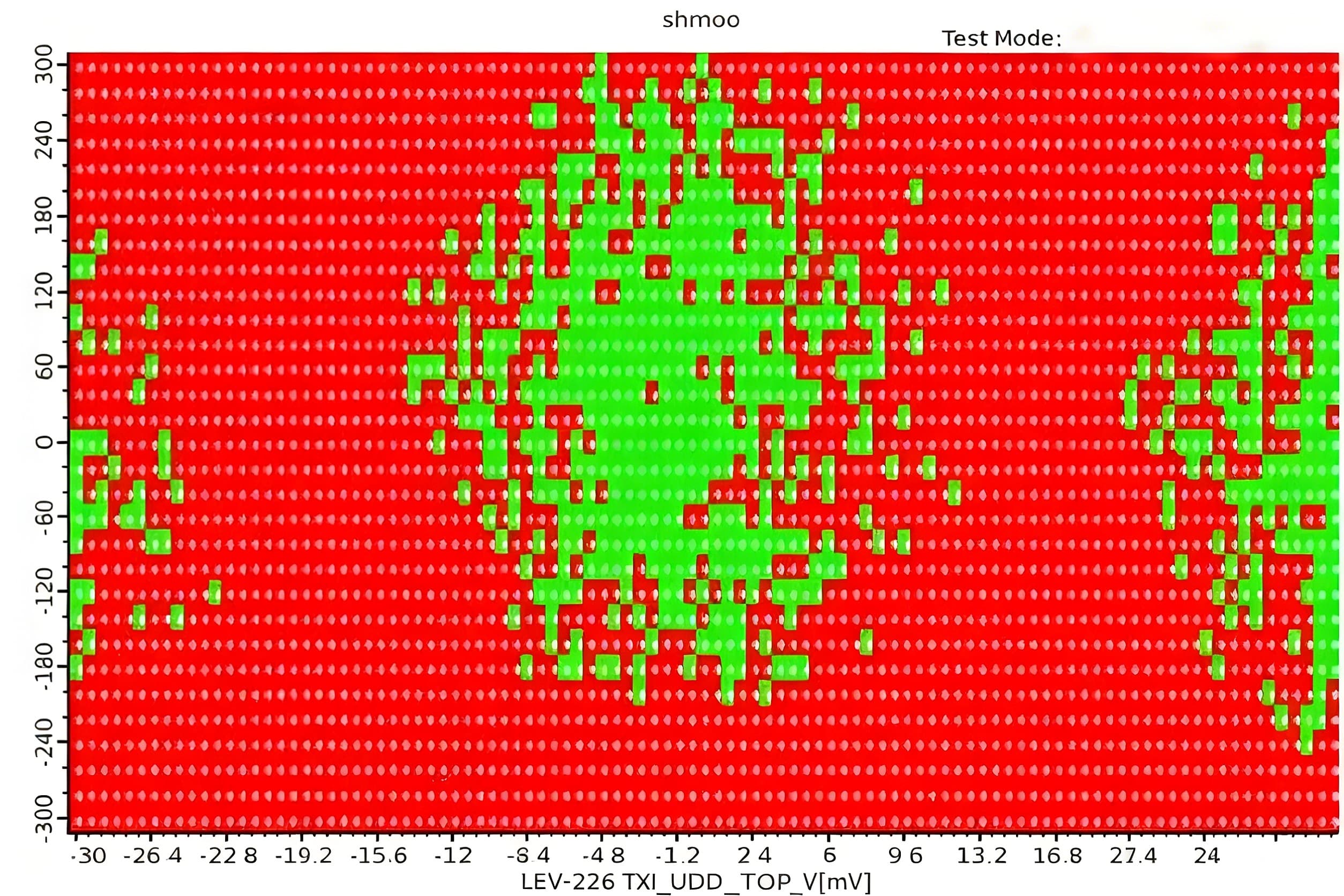
Figure: PLB eye diagram with RJ=1ps system clock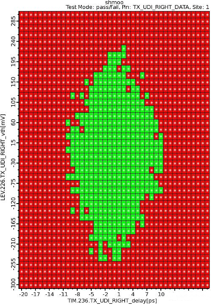
Figure: PLB eye diagram using JAM as reference clock
(3) Load Board Design
SerDes high-speed I/O interface testing imposes stringent signal integrity requirements on the peripheral circuits of transmit and receive pins. Even minor oversights can lead to significant errors in test results. We propose the following SI rules:
1) For the entire TX/RX link (including vias), TDR requirements are: single-ended impedance 50Ω ±5Ω, differential impedance 100Ω ±10Ω.
2) Account for packaging factors by ensuring equal attenuation between lanes, replacing the previous approach that only considered equal trace lengths on the load board.
3) For load board materials, prioritize low-dielectric-constant substrates such as Roger, Megtron6, or Necole. Lower dielectric constants result in reduced line loss and attenuation.
4) Implement high-speed routing requirements throughout the entire link (line width, spacing must meet specific ratios, signal ground processing, etc.).
5) After load board design completion, perform 3D simulation to meet requirements: S21 > -3dB @ 15GHz; S21 > -6dB @ 30GHz.
(4) Socket Selection
Sockets are a critical component in testing. There are two primary materials: pogo pins and conductive adhesive. Pogo pin sockets offer superior durability with minimal thermal variation, making them suitable for mass production. Conductive adhesive sockets exhibit low signal attenuation due to their manufacturing process characteristics, making them ideal for high-frequency testing. However, their lack of wear resistance prevents them from meeting mass production demands, limiting their use to characterization testing.
10.3 Test Results
Using the UDI solution, we conducted PRBS15 loopback testing on a 32 Gbps SerDes chip. The UDI test yielded an eye width of 19 ps and an eye height of 270 mV, which closely matched the DCA measurement results.
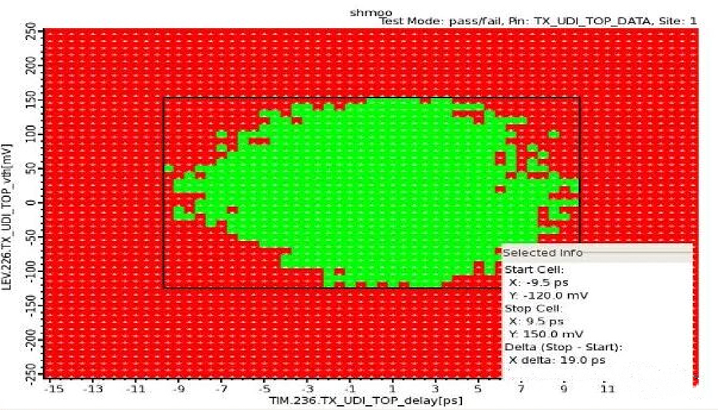
Figure: UDI Eye Diagram SHMOO Scan
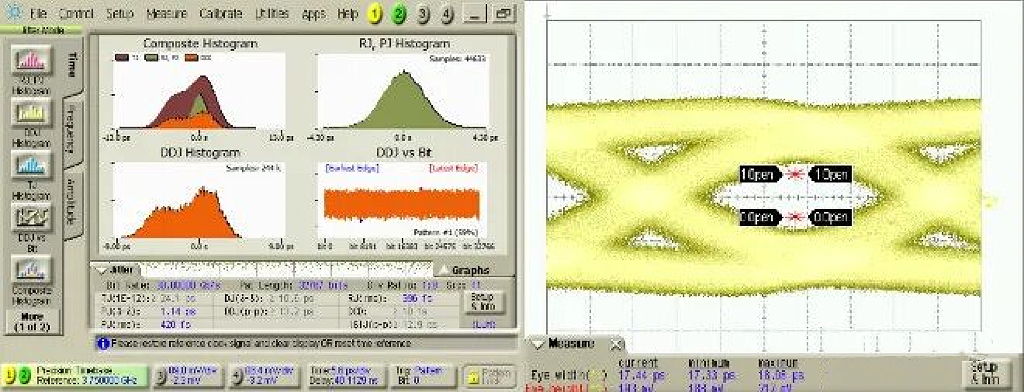
Figure: DCA Actual Measurement Results
10.4 Conclusion
The Nautilus UDI solution offers a comprehensive approach to automating high-speed I/O interface characterization and mass production testing. Since its launch, it has gained recognition from numerous domestic and international clients. Through collaboration with a leading domestic semiconductor company, it has enabled stable mass production of multiple 25–32 Gbps SerDes chips. We are confident that this solution will help more clients overcome the challenges of high-speed SerDes testing.
11. Maintenance & Troubleshooting
11.1 Root Cause Analysis and Targeted Solutions
|
Root Cause |
Issue Description |
Solution |
|
Signal Integrity (SI) |
Eye diagram failure, including: |
1. Adjust equalizer: |
|
Power Integrity (PI) |
Power supply noise couples into the SerDes analog circuitry, causing increased jitter. |
1. Measure power supply ripple: Use a power ripple probe to ensure it falls within the SerDes chip's specified range. |
|
Channel Fault |
Insertion loss, return loss, or crosstalk exceeding specifications, typically caused by physical damage or degradation. |
1. Measure S-parameters: Compare new and old channel performance using a VNA. |
|
Protocol and Configuration |
Configuration mismatches or compatibility issues at either end of the link. |
1. Check firmware/drivers: Update to the latest version. |
|
Environment and External Interference |
Intermittent issues caused by temperature fluctuations or external noise sources. |
1. Thermal Management: Verify heat dissipation and ensure chip operating temperature remains within specifications. |
(1) Prevention is better than a cure
Strictly adhere to SI/PI design specifications: Sound design is the foundation for stable operation.
Comprehensive Pre-Production Simulation: Fully predict performance before PCB manufacturing to avoid design flaws.
Compliance testing: Conduct rigorous standard compliance testing (e.g., PCI-SIG, IEEE) before productization.
(2) Establish a Healthy Baseline
When the system is functioning optimally, preserve "golden samples" of critical parameters—such as eye diagram snapshots, internal chip register configurations, and power supply noise levels—for future troubleshooting comparisons.
(3) Monitoring and Predictive Maintenance
Leverage SerDes chip-embedded diagnostic monitoring features (e.g., "channel health" indicators based on RX signal amplitude, temperature sensors, error counters) to enable real-time system status monitoring and early warning.