Switch Mode Power Supply Circuit Explained: Topologies, Design Tips & Expert Insights
1. Fundamentals & Background
In modern electronic devices, the selection and design of power supplies critically impact device performance and stability. Among these, Switch Mode Power Supplies (SMPS), as highly efficient and stable power solutions, are widely adopted across various electronic equipment.
1.1 What is SMPS and why is it used?
A switch-mode power supply, also known as a switching power supply or switching converter, is a high-frequency power conversion device that belongs to the category of power supplies. Its operating principle involves converting a single-level voltage into the voltage or current required by the user through various architectural configurations. Specifically, the SMPS uses an internal switching circuit to perform high-frequency chopping on the input voltage. This is followed by a filter circuit that removes high-frequency noise, ultimately delivering a stable DC voltage or current.
The input to an SMPS is typically an AC power source (such as utility power) or a DC power source, while the output provides the DC power required by electronic equipment. Within electronic devices, the SMPS plays the role of converting electrical energy from one form to another to meet the equipment's voltage and current requirements.
Switch-mode power supplies play a critical role in electronic devices, primarily manifested in the following aspects:
Voltage Conversion and Regulation: Switching power supplies convert input AC or DC power into the DC power required by the device and can adjust the voltage according to the device's needs. This enables their widespread application across various electronic devices, meeting the diverse power requirements of different equipment.
High Efficiency and Energy Savings: Compared to traditional linear power supplies, switching-mode power supplies offer higher conversion efficiency. Through high-frequency chopping and filter circuit designs, they achieve efficient utilization of input power while minimizing energy loss. This not only reduces device power consumption but also decreases heat generation, enhancing equipment stability and reliability.
Excellent Stability: Switching-mode power supplies maintain a stable output voltage. Through techniques like switching circuits and voltage regulation circuits, they sustain output stability even during significant input voltage fluctuations. This ensures regular device operation and prevents failures or damage caused by voltage variations.
Overload Protection: Switching-mode power supplies incorporate overload protection. When the device load exceeds capacity, the power supply automatically cuts off output current to prevent electronic equipment damage from overload. This protective feature ensures safe operation under abnormal conditions and extends equipment lifespan.
Noise Reduction and Filtering: Switching-mode power supplies typically incorporate internal noise reduction and filtering circuits that effectively suppress interference and noise in the input voltage. This enables them to deliver cleaner, more stable output power, enhancing device performance and stability.
1.2 Why do we need a switching-mode power supply?
Switching Mode Power Supplies (SMPS) form the cornerstone of modern electronic devices. Their necessity stems primarily from addressing several critical shortcomings of traditional linear power supplies.
Simply put, we need SMPS because it offers exceptional efficiency, compact size, lightweight design, and the ability to handle wide-range input-to-output voltage conversion efficiently. This makes it the ideal choice for nearly all modern electronic devices, from mobile phone chargers to data centers.
To better understand, we often compare it with another primary power supply type—the linear power supply.
Imagine a linear power supply as an adjustable faucet that achieves the desired water pressure by "blocking" excess flow. It uses a transistor (acting like a variable resistor) to "dissipate" excess voltage ((input voltage - output voltage) * output current), thereby converting high voltage to low voltage.
However, its efficiency is extremely low, with excess voltage wasted as heat. If the input-output voltage difference is significant, efficiency may fall below 50%. This not only consumes power but also requires massive heat sinks for cooling. Additionally, it is bulky and heavy due to the need for a mains frequency transformer (50/60Hz), which is inherently large and cumbersome.
In contrast, a switching power supply functions like a high-speed pump that precisely controls water flow through rapid switching and energy storage. It operates transistors in a switching state (either fully on with minimal resistance or entirely off with maximum resistance). By rapidly switching (tens of thousands to millions of times per second) and utilizing inductors and capacitors for energy storage and filtering, it achieves a stable output voltage.
Because the switching transistor has negligible resistance when conducting and nearly zero current when off, its power loss (P = I²R) is extremely low in both states. Efficiency easily reaches 80%-95% or higher. This translates to lower power consumption and reduced heat generation. Additionally, it utilizes high-frequency transformers and smaller inductors and capacitors. According to physics principles, higher frequencies require smaller magnetic cores and windings to deliver the same power. Consequently, SMPS can be designed to be highly compact and lightweight.
2. SMPS Working Principles and Topologies
2.1 How does a switch-mode power supply work?
Switch-mode power supplies (SMPS) abandon the traditional linear power supply's method of "consuming" excess energy. Instead, they efficiently convert voltage through high-speed switching, energy storage, and filtering. The core concept can be summarized as: rapidly turning the input power on and off (switching), storing the generated energy pulses, and finally smoothing and filtering them into a stable DC output.
Imagine you need to continuously fill a small cup (low-voltage output) from a large bucket (high-voltage input), while maintaining a steady flow of water in the cup.
Linear power supply approach: Connect a thin hose between the bucket and cup, carefully adjusting the valve to let water drip slowly and continuously into the cup. Most water is blocked by the valve, wasting energy and causing the valve to heat up (inefficient).
Switching Power Supply Approach:
Switch: Install a high-speed switching faucet between the bucket and cup.
Energy storage: Place a bucket (inductor) beneath the faucet.
Operation: Open the faucet rapidly for an instant, allowing a powerful surge of water to fill the bucket (energy storage). Then close it immediately.
Release: The moment the faucet closes, the bucket releases its stored water into the cup (energy release).
Filtering: Place a sponge (capacitor) beneath the cup to absorb the water flow's impact, maintaining a steady water level in the cup.
Regulation: An observer (control circuit) constantly measures the water level in the cup (output voltage). If the level drops, it increases the duration of each tap opening; if it rises, it reduces the opening time.
This process repeats tens of thousands of times per second. By precisely controlling the ratio of on-time (duty cycle) to off-time, a stable voltage is efficiently and accurately achieved.
The most basic buck SMPS includes the following key steps and components:
Step 1: Rectification (AC to DC)
Function: If the input is AC power (e.g., from a wall outlet), it is first converted into pulsating DC power via a diode bridge rectifier.
Step 2: Switching (Chopping - Critical Step)
Key Component: Switching Transistor, typically a MOSFET.
Action: Driven by a control chip (PWM controller), this switching transistor rapidly toggles between fully ON and entirely OFF states at extremely high frequencies (e.g., 50kHz - 1MHz).
Result: The smooth DC current is "chopped" into a series of high-frequency square-wave pulses.
Step 3: Energy Storage & Conversion
Key Components: Inductor and Diode.
Working Principle (Based on Buck Converter): When the switch is ON, Current flows through the inductor, supplying power to the load. Simultaneously, the inductor stores part of the electrical energy as magnetic energy. The diode is blocked due to reverse bias.
When the switch turns OFF: The inductor resists the sudden current drop (Lenz's Law), generating a reverse electromotive force (EMF) whose polarity reverses to maintain the current. This induced EMF flows through the diode (now forward-biased and conducting), forming a new path to release stored energy and continue powering the load.
Here, the diode is referred to as a freewheeling diode, providing a path for the inductor current to discharge when the switch turns off.
Step 4: Smoothing
Protagonist: Capacitor
Function: Although the current is relatively continuous after the inductor's freewheeling, the voltage remains pulsed. The role of a large-capacity output capacitor is to "smooth" these pulses. It charges during the pulses and discharges to the load during the pulse gaps, thereby producing a smooth, stable DC output voltage.
Step 5: Feedback & Regulation (The Brain)
Key Components: Feedback Circuit (Optocoupler or Sampling Resistor) and PWM Controller.
Process: The feedback circuit continuously samples the output voltage. This sampled value is compared against a precise reference voltage. If the output voltage is too high, the comparator signals the PWM controller; if too low, it sends another signal. Based on this error signal, the PWM controller dynamically adjusts the width of the pulse sent to the switching transistor (i.e., the duty cycle).
Output voltage too low? -> Increase the proportion of switch on-time (increase duty cycle) to deliver more energy.
Output voltage too high? -> Reduce the proportion of switch on-time (decrease the duty cycle), delivering less energy.
This process forms a closed-loop negative feedback system, ensuring remarkably stable output voltage under varying loads and input voltage fluctuations.
2.2 Common Topologies
(1) Buck Converter
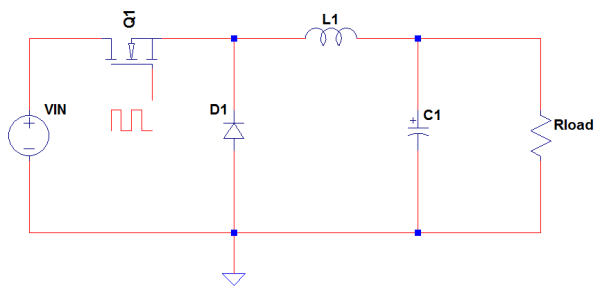
A buck converter is a step-down switching converter. In other words, its output is lower than its input. Buck converters are commonly used DC-DC converters, particularly suitable for automotive systems. They consist of a switch (MOSFET, BJT, or IGBT), a diode, an inductor, and an output storage capacitor. The switch is modulated by a PWM signal to achieve the target output voltage, ideally with zero switching losses.
Similar to a boost converter, the input and output voltages of a buck converter are determined by the duty cycle. The ideal duty cycle is:
Duty Cycle, Buck = Vout / Vin
Assuming an input voltage of 20V and an output of 5V, the duty cycle is 25%.
Buck Converter Operation During Switch On
When the switch is on, the diode is reverse-biased—the inductor charges. The capacitor also charges. At this time, the load's power demand is supplied by the input source.
Buck Converter Operation When the Switch is Off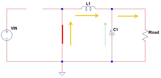
When the switch turns off, the inductor reverses polarity, causing the diode to become forward-biased. At this point, the load's power demand is supplied by the energy stored in the inductor and capacitor.
(2) Boost Converter

A boost converter consists of an inductor, a switch (MOSFET, BJT, or IGBT), a diode, and an output storage capacitor. The switch is modulated by a PWM signal to generate the desired output voltage in an ideal zero-loss manner.
A boost converter is a step-up DC-DC converter. In other words, its output is higher than its input. The output and input are determined by the duty cycle. The ideal duty cycle for a boost converter is
Duty Cycle, Boost = 1 – (Vin / Vout)
For example, with an output of 20V and an input of 5V, the duty cycle is 75%.
Boost converter operation during switch-on

When the switch turns on, the inductor charges. The diode becomes reverse-biased. The output capacitor supplies the required power to the load.
Boost Converter Operation When the Switch is Off
When the switch turns off, the inductor reverses polarity, causing the diode to become forward-biased. This allows the capacitor to recharge. At this point, the load's power demand is supplied by the input.
(3) Buck-Boost
A buck-boost converter combines a buck and a boost switching converter. It can operate with the output higher or lower than the input. There are two ways to implement buck-boost functionality: inverting and non-inverting. The anti-parallel buck-boost converter requires fewer components and is less expensive. Conversely, the parallel buck-boost converter uses more components and is more costly. If the operation is broken down into buck or boost modes, the analysis for a parallel buck-boost converter may resemble that of buck and boost topologies. However, the analysis for an anti-parallel buck-boost converter differs.
(4) Flyback/Forward
① Forward Switching Power Supply
Forward-conversion switching power supplies feature relatively complex structures but deliver high output power, making them suitable for 100–300W applications. They are commonly used in low-voltage, high-current switching power supplies and enjoy widespread adoption.
As shown below, in a forward switching power supply, when the switch is turned on, the output transformer acts as a medium for direct magnetic coupling of energy. Electrical and magnetic energy are converted simultaneously, enabling both input and output to occur concurrently. However, practical applications reveal limitations: additional back-EMF windings are required (to prevent back-EMF from the primary coil from damaging the switch transistor), and an extra secondary inductor is needed for energy storage and filtering. Consequently, forward-converter designs incur higher costs compared to flyback converters, and their transformers are bulkier.

② Flyback Switching Power Supply
As shown below, a flyback switching power supply employs a flyback high-frequency transformer to isolate the input and output circuits. This transformer not only converts voltage and transmits energy but also functions as an energy storage inductor, making its design similar to that of an inductor. The overall circuit is relatively simple and easy to control, making flyback designs widely used in low-power applications ranging from 5 to 100W. In a flyback switching power supply, when the switch turns on, the primary inductor current in the transformer rises. Since the output coil of the flyback circuit has opposite polarity, the output diode turns off. The output capacitor supplies energy to the transformer, which in turn stores it, and then to the load. When the switch turns off, the induced voltage in the primary inductor reverses. At this point, the output diode conducts, supplying power from the transformer to the load through the diode while simultaneously charging the capacitor.
Comparing the two, the forward converter's transformer serves only as a transformer, functioning as a buck circuit with an integrated transformer. The flyback converter's transformer acts as an inductor with transformer capability, forming a buck-boost circuit. In summary, forward and flyback operate differently: in forward, both primary and secondary work; in flyback, the secondary works while the primary is off, with a freewheeling inductor providing current continuity. Forward typically operates in CCM mode with a generally lower power factor, where input/output voltage and duty cycle ratio are proportional. In a flyback operation, the primary works while the secondary remains inactive, with both sides isolated. It typically operates in DCM mode. However, the transformer's inductance is relatively low, and an air gap is required, making it generally suitable for small to medium power applications.
Forward transformers are idealized as non-energy-storage devices. However, due to finite excitation inductance, excitation currents cause core enlargement. To prevent magnetic saturation, auxiliary windings are required for flux reset. The flyback transformer's operation can be viewed as a coupled inductor, where energy is first stored and then released. Since the input and output voltages of the flyback transformer have opposite polarities, the secondary can provide a reset voltage to the core after the switch turns off. Therefore, the flyback transformer does not require an additional magnetic flux reset winding.
(5) Push-Pull/Inverting
① Push-Pull

The FETs are driven out of phase, employing pulse width modulation (PWM) to regulate the output voltage.
Excellent transformer core utilization—power is transferred during both half-cycles.
Full-wave topology, so the output ripple frequency is twice the transformer frequency.
The voltage applied to the FET is twice the input voltage.
② Inverting
Common flyback-based topologies in switching power supplies primarily include the following two categories:
The core feature of the Flyback topology is the phase inversion between the input and output voltages, achieved through the reverse winding configuration of the transformer's primary and secondary coils to enable energy conversion. When the switch turns off, the secondary winding releases magnetic field energy. This topology is generally suitable for scenarios requiring significant input-output voltage differences and isolation, such as battery-powered devices.
The Buck-Boost topology's core feature is its ability to both step up and step down voltage, with the output voltage phase inverted relative to the input. Its operation involves periodic switching of the power switch, combined with inductors and diodes, to achieve voltage conversion. It is suitable for scenarios with a wide input-output voltage range, but note that the floating power switch may increase driver circuit complexity.
Flyback and Buck-Boost represent typical inverting topologies in switching power supplies. The former achieves isolation through transformer winding inversion, while the latter employs circuit design to reverse the input-output voltage phase. Selection requires balancing performance and complexity based on specific requirements.
2.3 Isolated vs Non-Isolated SMPS
(1) Concepts and Characteristics of Isolated and Non-Isolated Power Supplies
Isolated Switching Power Supply
Isolated switching power supplies require high-frequency transformers for DC-DC conversion. Input and output are physically isolated via the transformer, offering enhanced safety.
The input AC power is rectified and filtered by a rectifier bridge to produce high-voltage DC. The SMPS control chip then converts this high-voltage DC into high-frequency pulsating DC, which is fed into the primary winding of the high-frequency transformer. Through electromagnetic induction, the secondary winding of the high-frequency transformer produces low-voltage pulsating DC. This low-voltage pulsating DC is subsequently rectified and filtered to yield the final DC output.
The switching power supply control chip automatically adjusts the switching frequency and duty cycle based on output voltage and current requirements, achieving high energy conversion efficiency.
Non-isolated Switching Power Supply
Non-isolated switching power supplies lack the physical isolation provided by a transformer, with the input and output terminals connected at one end.
Without a high-frequency transformer, non-isolated switching power supplies directly convert high-voltage DC to low-voltage DC through high-speed switching control. During this conversion process, the switching power supply control chip experiences significant voltage drops, limiting the achievable output current.
Typically, the output current of this type does not exceed 300mA. It is generally used in applications that require low output current, a compact size, and a low cost.
The high-frequency ferrite transformer in switching power supplies is a critical component for high-frequency energy conversion.
The core material used in switching power supplies is ferrite, whereas conventional silicon steel sheets suffer from excessive losses at high frequencies, making them unsuitable for high-frequency operating conditions.
The BD1 bridge rectifier rectifies the 220V AC input and then stabilizes it to approximately 300V DC through the pi-filter, composed of C1, L1, and C2. The series resistors R2 and R3 supply a weak startup current to pin 3 (INV), establishing the oscillation frequency to control MOSFET conduction.
Additionally, once oscillation is established, an auxiliary winding on the primary provides a stable drive current to control the MOSFET continuously.
(2) Comparative Analysis of Isolated and Non-Isolated Power Supplies
Based on the above concepts, common non-isolated power supply topologies include Buck, Boost, and Buck-Boost converters. Isolated power supplies primarily utilize various topologies with isolation transformers, such as Flyback, Forward, Half-Bridge, and LLC converters.
By comparing standard isolated and non-isolated power supplies, we can intuitively identify their respective advantages and disadvantages, which are largely complementary.
(3) Application Scenarios for Isolated and Non-Isolated Power Supplies
Understanding the strengths and weaknesses of isolated and non-isolated power supplies reveals their respective advantages. For common embedded power supply choices, we can make precise judgments:
For front-end system power supplies, isolated power is generally used to enhance interference resistance and ensure reliability.
For powering ICs or specific circuits within a PCB, non-isolated solutions are preferred based on cost-effectiveness and space constraints.
In safety-critical applications, such as AC-DC converters connected to mains power or medical power supplies, isolated power supplies are mandatory to ensure personal safety. In some cases, reinforced isolation power supplies are also required.
For remote industrial communication powering, isolated power supplies are generally used to supply each communication node individually, effectively reducing the impact of ground potential differences and wire coupling interference.
For battery-powered applications with stringent endurance requirements, non-isolated power supplies are employed.
2.4 Power Factor Correction & EMI Filtering
(1) Power Factor Correction
PFC (Power Factor Correction) primarily controls the input current waveform to synchronize it with the input voltage waveform. This improves the power factor, reduces harmonic content, and resolves electromagnetic interference (EMI) and electromagnetic compatibility (EMC) issues caused by severe current waveform distortion from capacitive loads. Power factor represents the ratio of active power to apparent power (total power consumption). A higher power factor indicates greater electrical efficiency. Switching power supplies employ capacitive input circuits where phase differences between current and voltage cause reactive power losses.
AC and voltage are in phase with a purely resistive load, meaning resistors are power-dissipating devices. With a strictly capacitive load, the current leads the voltage by 90°. With a purely inductive load, the voltage leads the current by 90°. Both inductors and capacitors are power-storing devices.
Currently, PFC includes passive PFC (passive PFC) and active PFC (active PFC).
Passive PFC has two types: one is inductive compensation, which adds an inductor (with appropriately selected inductance) between the rectifier bridge and filter capacitor. Its principle is to use the inductor to reduce the phase difference between the fundamental current and voltage of the AC input, thereby improving the power factor. The other is the valley-filling circuit type. Its principle involves using a valley-filling circuit after the rectifier bridge to increase the conduction angle of the rectifier diodes. By filling the valley points, the input current is transformed from a spiked pulse waveform into one closer to a sine wave. Compared to inductive compensation, this circuit offers the advantage of simplicity while providing effective power factor correction.
Active PFC consists of inductors, capacitors, and associated components. It employs dedicated ICs to adjust the current waveform and compensate for the phase difference between current and voltage. An active PFC can serve as an auxiliary power supply and produce very low ripple in its output DC voltage.
(2) EMI Filtering
In switching power supplies, EMI filters play a significant role in suppressing both common-mode and differential-mode conducted noise. Building upon the fundamental principles of filtering, this study explores a method for independently analyzing and modeling common-mode and differential-mode signals. Ultimately, based on this approach, a design procedure for EMI filters is proposed.
High-frequency switching power supplies have gained widespread adoption across industrial, defense, and consumer electronics sectors due to their advantages in size, weight, power density, and efficiency. When applied to AC grids, the rectifier circuit often causes discontinuous input currents, significantly reducing input power factor while generating substantially higher-order harmonics. Simultaneously, the high-speed switching operations of power transistors within these supplies (ranging from tens of kHz to several MHz) create sources of electromagnetic interference (EMI). Published research indicates that the primary interference forms in switching power supplies are conducted interference and near-field radiated interference. Conducted interference can also be injected into the grid, disrupting other connected equipment.
Numerous methods exist to reduce conducted interference, such as:
-Proper grounding layout, including star-shaped grounding to avoid looping and minimize standard impedance
-Designing appropriate buffer circuits
-Reducing stray capacitance in circuits
Additionally, EMI filters can be employed to attenuate mutual noise interference between the power grid and the switching power supply.
EMI disturbances are often difficult to characterize precisely, so filter design typically involves iterative calculations and prototyping to meet design requirements progressively.
3. Key Design Considerations
3.1 Selecting MOSFETs, Diodes & Inductors
① MOSFET Selection
The first step in selecting power MOSFETs: P-channel or N-channel?
Power MOSFETs come in two types: N-channel and P-channel. When selecting between N-channel and P-channel devices during system design, the choice must be made based on the specific application requirements. N-channel MOSFETs offer a wider range of available models and lower cost; P-channel MOSFETs have fewer model options and a higher price. If the source terminal voltage of a power MOSFET is not connected to the system reference ground, N-channel devices require a floating ground power supply drive, transformer drive, or bootstrap drive, resulting in complex drive circuits. P-channel devices can be directly driven, offering simpler drive configurations.
Key applications requiring consideration of N-channel versus P-channel include:
CPU and system cooling fans in laptops, desktops, and servers; motor drives for printer paper feed systems; motor control circuits in home appliances like vacuum cleaners, air purifiers, and electric fans. These systems employ full-bridge circuit configurations where either P-channel or N-channel MOSFETs can be used in each bridge arm.
In communication systems with 48V input, hot-swap MOSFETs placed at the high side can use either P-channel or N-channel devices.
Two back-to-back power MOSFETs in series within the laptop input circuit, serving as reverse-connection protection and load switches. N-channel MOSFETs require an internal charge pump driver integrated within the control chip, while P-channel MOSFETs can be directly driven.
Selecting the Package Type
After determining the channel type of the power MOSFET, the next step is to select the package. The principles for package selection are:
Temperature rise and thermal design are the most fundamental requirements for package selection.
Different package sizes exhibit varying thermal resistance and power dissipation. Beyond considering system cooling conditions and ambient temperature—such as the presence of air cooling, heat sink shape/size constraints, and enclosure type—the fundamental principle is to select a power MOSFET with more universal parameters and packaging while ensuring acceptable temperature rise and system efficiency.
Sometimes, due to other constraints, multiple MOSFETs must be connected in parallel to address thermal issues. This approach is common in applications like PFC, electric vehicle motor controllers, and secondary synchronous rectification in communication system module power supplies.
If parallel connection is not feasible, options include selecting higher-performance power MOSFETs or adopting larger or novel packaging formats. For instance, in certain AC/DC power supplies, transitioning from TO220 to TO247 packaging, or in communication system power supplies, utilizing the new DFN8*8 package.
System Size Constraints
PCB dimensions and internal height limitations constrain specific electronic systems. For instance, module power supplies in communication systems typically use DFN5*6 or DFN3*3 packages due to height restrictions. In some AC/DC power supplies, ultra-thin designs or enclosure limitations necessitate mounting TO220-packaged power MOSFETs with pins bent flat to the base during assembly, precluding the use of TO247 packages.
Ultra-thin designs sometimes involve bending device pins flat, which complicates manufacturing processes.
In the design of high-capacity lithium battery protection boards, due to extremely stringent size constraints, chip-scale CSP packages are now predominantly used to maximize thermal performance while ensuring the smallest possible dimensions.
Cost Control
Early electronic systems predominantly used through-hole packages. In recent years, rising labor costs have prompted many companies to switch to surface-mount packages. Although surface-mount soldering costs exceed through-hole methods, the high automation of surface-mount processes keeps overall costs within reasonable limits. In cost-sensitive applications like desktop motherboards and PC cards, DPAK-packaged power MOSFETs are typically chosen for their low cost.
Therefore, when selecting a power MOSFET package, companies should consider their own corporate style and product characteristics while comprehensively evaluating the factors mentioned above.
Selecting the on-resistance (RDSON): Note that this is not the current.
Engineers often focus on RDSON because it directly correlates with conduction losses. A lower RDSON results in reduced conduction losses, higher efficiency, and lower temperature rise for the power MOSFET.
Similarly, engineers often prioritize reusing existing components from previous projects or the parts library, without giving much thought to the actual selection method for RDSON. When the selected power MOSFET exhibits excessively low temperature rise, cost considerations may lead to switching to a component with a higher RDSON. Conversely, if the power MOSFET's temperature rise is too high and system efficiency is low, engineers may switch to an element with a lower RDSON or adjust by optimizing the external drive circuit or improving heat dissipation methods.
For a completely new project with no prior reference, how should the RDSON of the power MOSFET be selected? Here's one method: the power distribution approach.
When designing a power supply system, known parameters include: input voltage range, output voltage/output current, efficiency, operating frequency, drive voltage, and other technical specifications. The key parameters related to the power MOSFET are primarily these. The steps are as follows:
Calculate the system's maximum power dissipation based on the input voltage range, output voltage/current, and efficiency.
Make rough estimates for stray losses in the power loop, static losses in non-power loop components, IC static losses, and driver losses. Empirically, these can account for 10%–15% of total losses. If the power loop includes a current-sensing resistor, calculate its power dissipation. Subtract these losses from the total loss to obtain the remaining power loss from the power devices, transformer, or inductor. Distribute this residual power loss proportionally between the power devices and the transformer/inductor. If uncertain, allocate it equally among the components to determine the power loss per MOSFET.
Allocate the MOSFET's power loss proportionally between switching loss and conduction loss. If uncertain, distribute equally between switching and conduction losses.
Calculate the maximum allowable on-resistance based on the MOSFET's conduction loss and the effective current flowing through it. This resistance represents the MOSFET's RDSON at its maximum operating junction temperature. The RDSON value listed in the datasheet for power MOSFETs is specified under defined test conditions and varies under different definitions. The test temperature is TJ=25°C. Since RDSON exhibits a positive temperature coefficient, calculate the corresponding RDSON at 25°C based on the MOSFET's maximum operating junction temperature and RDSON temperature coefficient, using the calculated RDSON value above.
Select a suitable power MOSFET model based on the RDSON at 25°C, then adjust the actual RDSON parameter of the MOSFET up or down accordingly.
Through the above steps, the power MOSFET model and RDSON parameters are preliminarily selected.
② Diode Selection
Application Scenario Matching
Rectification: Select high-voltage, high-current diodes (e.g., 1N5408).
High-Frequency Switching: Select diodes with short Trr and low Cj (e.g., Schottky or fast recovery diodes).
Voltage Regulation: Select a Zener diode with a VZ matching circuit requirements, ensuring sufficient current margin.
Protection: Select TVS diodes with VBR slightly exceeding the circuit's operating voltage.
Key Parameter Verification
Forward Voltage Drop (Vf): Affects efficiency; select Schottky diodes for low-voltage applications.
Reverse Voltage Rating (VRM): Must be ≥1.2 times the circuit's maximum reverse voltage.
Reverse Recovery Time (Trr): Must be <10ns for high-frequency applications to minimize switching losses.
Junction Capacitance (Cj): Select Cj < 5 pF in high-frequency circuits to minimize signal distortion.
Thermal Design and Reliability
Junction Temperature Control: Calculate junction temperature Tj = Ta + (P_loss × Rθja) to ensure Tj ≤ maximum rating (150°C for silicon devices).
Derating: Design voltage and current parameters at 80% of rated values.
Package Selection: For high-current applications, choose packages with heat sinks like TO-220.
General Applications and Safety Certifications
Select standard models (e.g., 1N4148) for general applications; choose Schottky/TVS diodes for high-performance requirements.
Prioritize suppliers with safety certifications (UL, TUV, etc.).
③ Inductor Selection
Inductance
As a fundamental parameter, selecting the appropriate inductance value is paramount. Inductance serves as the basic unit for measuring a coil's storage capacity. Standard units include H, uH (microhenry), and nH (nanohenry), analogous to capacitance units (uF, nF, etc.). While "Henry" is the Chinese term for H, units with uH and nH are more prevalent in PCB design.
What factors influence the inductance value? Generally, inductance is affected by the number of coil turns, coil length, cross-sectional diameter, and the magnetic permeability of the core material, among other factors.
Inductance formula: L = (N² * μ * A) / l
L represents the inductance value (in henries, H)
N represents the number of turns in the coil
μ represents magnetic permeability (units: henries per meter, H/m)
A represents the cross-sectional area of the coil (in square meters, m²)
l represents the length of the coil (in meters, m)
Although these factors influence inductance, the specific inductance value cannot generally be directly calculated using formulas for these variables. This is because actual production or material fabrication involves numerous complex factors. Therefore, inductance is typically determined through direct measurement using instruments.
Additionally, the magnetic permeability of core materials varies with frequency. As frequency increases or decreases, the current distribution within the coil changes accordingly. Other factors may also alter the equivalent dimensions of the inductor, thereby modifying magnetic flux and consequently changing the inductance value.
Therefore, manufacturers typically specify in their technical specifications the frequency at which the inductance value was measured. As shown in the diagram below, the inductance value gradually decreases as the frequency increases.
Accuracy
Accuracy refers to the corresponding error margin, indicating the possible deviation range between the actual value and the nominal value. Generally, inductors in the μH range can achieve accuracy between ±5% and ±30%, while those in the nH range can be precise to ±0.1nH. When selecting inductors, a comprehensive choice can be made based on requirements and cost considerations.
Among conventional inductors, air-core coil inductors typically exhibit higher inductance accuracy than iron-core inductors (since air-core inductors lack the saturation effect of magnetic materials, their inductance values remain relatively more stable).
Direct Current Resistance (DCR)
Represents the resistance value of the inductor itself under DC conditions. This primarily affects operational losses. Under normal circumstances, a lower DCR is preferable, as it indicates better conductivity and reduced losses. Therefore, prioritize selecting inductors with lower DCR during selection.
What factors primarily influence DCR? It is mainly related to inductance, rated current, and packaging. DCR can be as low as the milliohm range or as high as several ohms.
Is there any relationship between these factors? Essentially, DCR can be viewed as a parasitic parameter. The specific relationship is as follows:
a. For identical inductance values, larger packaging dimensions result in higher DCR.
b. For identical package sizes, higher inductance values result in greater DCR.
c. For identical inductance values, inductors without magnetic shielding exhibit higher DCR than those with shielding.
3.2 PCB Layout & Thermal Management
PCB layout and thermal management are critical for the stable, efficient, and reliable operation of Switching Mode Power Supplies (SMPS). Poor design can lead to noise, oscillations, severe electromagnetic interference (EMI), or even direct failure; inadequate thermal management significantly reduces efficiency and lifespan.
(1) Core Layout Principles (The Golden Rules)
These principles form the foundation of all excellent SMPS layouts.
① Minimize high-frequency loop area
Objective: This is the most critical principle. All fast-switching (high-frequency) current paths act as "antennas," radiating EMI and inducing noise.
Critical loops:
Power Loop: Input capacitor → Switching transistor (MOSFET) → Transformer/inductor → Output capacitor → Ground → Return to input capacitor. This loop experiences an extremely high current rate of change (di/dt) and must be minimized.
Gate Drive Loop: Controller drive pin → Gate resistor → MOSFET gate → MOSFET source → Return to controller ground. This loop experiences a highly high voltage rate of change (dv/dt), making it prone to noise coupling.
② Implement a single ground point
Objective: Prevent mixing of noisy power ground (high-current ground) with clean signal ground (controller feedback ground), which can introduce ground plane noise affecting control signal stability.
Method: Typically, the ground terminals of input/output capacitors serve as the "power ground star point." The controller's ground pin and the feedback network's ground connect to the "signal ground star point." Finally, a thick trace or a 0-ohm resistor/choke connects the two star points.
③ Keep sensitive traces away from noise sources
Sensitive nodes: Feedback networks (voltage divider resistors, compensation networks), current sensing signals, enable/soft-start pins.
Noise Sources: Switching nodes (SW node, i.e., connection points of MOSFETs, inductors, diodes), transformers, inductors, and any high-current traces.
Method: Route sensitive traces away from these noise sources. Avoid routing beneath or parallel to them. Use ground planes when necessary.
(2) Specific Layout Techniques and Steps
Step 1: Component Placement
Define power paths first: Like planning a highway, place power components (input capacitors, switching transistors, inductors/transformers, output capacitors, rectifier diodes) first. Ensure their physical positions are compact, with the shortest and most direct connection paths.
Place input capacitors adjacent to switching transistors: Input capacitors (especially high-frequency decoupling ceramic capacitors) must be extremely close to the MOSFET's drain and source pins. This is critical for minimizing the power loop area.
Place bypass capacitors adjacent to the controller: The controller's VCC bypass capacitors must be positioned immediately next to its power supply and ground pins.
Position feedback networks: Place feedback resistors and compensation networks near the controller, away from noise sources.
Consider thermal management: Reserve sufficient space and thermal paths for high-power components (MOSFETs, diodes, inductors).
Step 2: Routing
Keep power traces short and wide: Use large-area copper pours (Polygon Pour) for high-current paths to minimize DC resistance and inductance. Use 45° angles or arcs for trace corners; avoid 90° right angles.
Keep switch nodes (SW) small: SW nodes exhibit the highest dv/dt noise. Their copper area should be sufficiently large to carry current but not excessively large to prevent acting as radiating antennas.
Feedback traces should be short and direct: The key is to keep them away from noise sources. Ideally, route them on quiet inner layers, shielded on both sides by ground traces (Guard Traces). The feedback point should be taken directly from the output capacitor terminals, not from the inductor or diode pins.
Ground plane treatment: Ideally, use a full ground plane. If unfeasible, employ a "ground grid" or large copper pour to connect grounds. Provide low-inductance ground connections for critical components (e.g., input capacitors, controllers). Place ground vias at multiple PCB locations, especially along high-current ground paths.
Step 3: Stack-up Design
A 4-layer board offers the best cost-performance ratio:
Top Layer: Signals and power components
Mid-Layer 1: Full ground plane (Critical! Provides shielding and low-inductance return paths)
Mid-Layer 2: Power plane (or additional routing layer)
Bottom Layer: Signals and routing
2-layer boards present greater challenges: They require more careful use of large copper pours as ground planes and ensuring critical loop areas are minimized.
(3) Thermal Management
Heat is the primary cause of power supply failures. Heat primarily originates from switching losses and conduction losses in MOSFETs, conduction losses and reverse recovery losses in diodes, and iron losses and copper losses in magnetic core components.
① Identify heat sources and calculate losses
First, estimate power dissipation for major components using formulas from device datasheets.
② Utilize the PCB as a heat sink
Large copper pads: Reserve as much copper area as possible for the pads of heat-generating components.
Thermal vias: This is the most critical heat dissipation method in multilayer boards.
Place an array of thermal vias beneath the pads of heat-generating components (e.g., MOSFETs, diodes).
The vias conduct heat from the top layer to the inner ground plane and bottom layer, utilizing the entire PCB for heat dissipation.
Typical Design: Use 0.3mm diameter vias with 1.0mm-1.2mm pitch.
Solder Mask Opening: Remove the solder mask (open window) in areas requiring additional soldered thermal contact to facilitate soldering or thermal paste application.
③ Add External Heat Sinks
When PCB-only cooling is insufficient, aluminum heat sinks must be added for MOSFETs and diodes.
Ensure good contact between the heat sink and component surface by filling air gaps with thermal grease.
Secure using clips, screws, or adhesive.
④ Utilize Airflow
When designing the layout, consider the airflow direction within the product (natural convection or fan-forced cooling) and position heat-generating components along the airflow path.
Avoid placing heat-generating components in dead zones or areas with no airflow.
⑤ Thermal Simulation
For high-power designs or those with stringent reliability requirements, perform thermal simulation using EDA tools (e.g., ANSYS Icepak, Siemens FloTHERM) or online tools to identify hotspots early and optimize layout.
3.3 Control Loop & Stability
The core of a Switching Mode Power Supply (SMPS) involves rapidly switching power transistors (e.g., MOSFETs) to convert input electrical energy into high-frequency pulses. These pulses are then smoothed into a stable DC output through a filter composed of inductors and capacitors.
However, the real world is dynamic:
Load variations: Connected devices may experience sudden increases or decreases in power consumption (e.g., a CPU transitioning from idle to full load).
Input variations: Input voltage may fluctuate (e.g., battery voltage drop or grid fluctuations).
Component tolerances: Inductors, capacitors, and other components exhibit measurement errors and temperature drift.
Without control, the output voltage would fluctuate wildly with these changes, failing to meet the demands of connected devices. Thus, the control loop was born. Its sole purpose is to maintain a stable, precise output voltage regardless of input voltage or load variations.
Stability refers to the control loop's ability to smoothly, rapidly, and oscillation-free readjust the output voltage to the target value when facing disturbances, rather than entering self-oscillation that causes system collapse.
A typical negative feedback control loop comprises the following main components:
(1) Sampling Network (Feedback Network)
Typically, a simple resistive voltage divider proportionally reduces the output voltage Vout to generate a sampling voltage Vfb that is directly proportional to the output voltage.
For example, if the target output is 12V and the voltage divider ratio is 1/4, then Vfb is 3V.
(2) Error Amplifier (EA)
It compares the sampling voltage Vfb with a highly stable reference voltage Vref (e.g., 2.5V).
It outputs an error voltage Vcomp (or Veao), whose value is proportional to the difference (Vref - Vfb).
If Vout decreases → Vfb decreases → (Vref - Vfb) increases → Vcomp increases.
This is a critical control signal.
(3) Compensation Network
This is the heart of the loop design, typically composed of resistors and capacitors connected around the error amplifier.
Its function is to "shape" the error signal Vcomp, introducing appropriate gain and phase characteristics to ensure overall loop stability. It determines the dynamic response performance of the loop (speed, overshoot, and damping).
Typical structures include: Type I, Type II, and Type III compensators, with increasing complexity.
(4) Modulator & Power Stage
Modulator: Typically a PWM controller. It compares the compensated voltage Vcomp with a triangular wave (sawtooth wave) to generate a pulse signal with a variable duty cycle (D). The higher the Vcomp, the larger the duty cycle.
Power Stage: Includes switching transistors, driver circuits, inductors (L), capacitors (C), diodes/synchronous MOSFETs, etc. It transfers input power to the output based on the PWM signal's duty cycle.
This section inherently introduces gain and phase delay (e.g., an LC filter is a second-order system that introduces 180° phase lag).
Engineers typically use frequency domain analysis to evaluate stability mathematically. The most fundamental tool is the Bode plot.
The Bode plot consists of two diagrams:
Amplitude-Frequency Response Plot: Shows the magnitude of the loop gain T(s) (in dB) as a function of frequency.
Phase-frequency characteristic diagram: Shows the curve of the phase (in degrees) of the loop gain T(s) as a function of frequency.
From the Bode plot, we can read two critical metrics:
① Gain Crossover Frequency (fgc):
The frequency on the amplitude-frequency curve at which the gain is 0 dB.
This represents the loop's response speed. A higher fgc indicates faster response to load or input changes. However, it is constrained by the switching frequency (typically, fgc should be less than 1/5 to 1/10 of the switching frequency).
② Phase Margin (PM):
The number of degrees remaining on the phase curve to reach -180 ° at the gain crossover frequency (fgc).
PM > 0 is a necessary condition for system stability.
The magnitude of PM determines the system's stability and dynamic response:
PM > 45° (typically required between 45°-60°): Stable. Response exhibits no overshoot or only slight overshoot, achieving smooth stabilization.
PM < 45°: Underdamped. Response exhibits significant overshoot and oscillation, requiring an extended time to stabilize.
PM ≈ 0°: Critically stable. The system exhibits sustained oscillation with constant amplitude.
PM < 0°: Unstable. Oscillations with increasing amplitude until system collapse.
③ Gain Margin (GM):
The value by which the gain falls below 0 dB at the frequency where the phase reaches -180°.
Typically requires GM > 10 dB. This represents another safety margin ensuring stability.
A well-designed loop should possess a sufficiently high crossover frequency (fast response) while maintaining a phase margin exceeding 45° and a gain margin exceeding 10 dB.
4. How to Use and Test SMPS Power Supply
4.1 Selection Process & Specs Validation
Generally, we only consider purchasing a switching power supply when our existing product malfunctions. You can directly take the previous power supply to professional switching power supply distributors to inquire about available models matching the original specifications or compatible alternatives. The process can be approached from the following aspects:
(1) Switching Power Supply Input and Output Types
Primarily categorized as: ① AC/DC ② DC/DC ③ DC/AC Note: AC denotes alternating current, DC denotes direct current. For example, AC/DC indicates AC input with DC output.
(2) Input Voltage
Standard input voltage specifications include 110V, 220V, and universal input voltage (AC: 85V–264V). Select the input voltage specification based on the region of use.
(3) Output Voltage and Current Selection
When selecting a switching power supply, the voltage must match first, followed by the current. The rated current of the switching power supply must exceed the maximum current of the load. For example, if your circuit requires 15V and 60mA, it is generally recommended to choose a power supply rated at 100mA or higher. Additionally, as long as the voltage matches, regardless of how much higher the current provided by the switching power supply is than the actual usage, the circuit will only draw the required amount and will not be damaged.
(4) Switching Power Supply Functions
① Regulated Switching Power Supply: Both input and output voltages are rated at specific values;
② Thyristor Switching Power Supply: Output voltage can be adjusted by modifying the input voltage.
③ Adjustable Switching Power Supply: Within the rated input voltage range, both output voltage and current can be regulated via potentiometers or similar methods.
(5) Switching Power Supply Load Characteristics
To enhance system reliability, it is recommended that the switching power supply operate at 50%-80% load. Select a model with approximately 30% higher rated output power than the actual requirement. For example, if the required power is 20W, choose a switching power supply with an output power rating of 25W-40W. If the load is a motor, light bulb, or capacitive load that draws high current during startup, select an appropriate power supply to prevent overload.
(6) Ambient Temperature
Consider the operating ambient temperature of the switching power supply and whether additional auxiliary cooling equipment is available. At excessively high ambient temperatures, the power supply must derate its output. Refer to the derating curve for output power versus ambient temperature.
4.2 Wiring & Safety Note
The input voltage for the switching power supply can be either 220V or 110V. Select the input voltage rating appropriately based on the circuit design. Failure to do so may damage the switching power supply.
Distinguish between the ground terminal and neutral terminal on the output voltage terminals of the switching power supply. Ensure the power supply is reliably grounded.
The metal casing of the switching power supply is typically connected to ground (FG). Ensure it is reliably grounded for safety. Do not mistakenly connect the casing to the neutral line.
Before energizing the power supply after installation, thoroughly recheck and verify all terminal connections. Confirm that input/output, AC/DC, single-phase/multi-phase, positive/negative polarity, voltage ratings, and current ratings are all correct and unambiguous before energizing.
High-power switching power supplies typically feature two or more "+" output terminals and "-" output terminals. These terminals actually belong to the same output electrode internally; multiple terminals are provided for user wiring convenience and are internally connected in parallel.
To ensure adequate heat dissipation, switch-mode power supplies should be installed in locations with good air convection or mounted on equipment enclosures to transfer heat to the exterior through the casing.
Switching power supplies are tested with resistive loads before shipment. If intended for capacitive or inductive loads, this must be specified in the purchase contract beforehand.
For dual-output switch-mode power supplies with symmetrical loads, prioritize symmetrical output power supplies.
For users with FG grounded, a slight tingling sensation when touching the casing or output is normal. When floating, FG outputs approximately 110V AC to ground, a characteristic determined by the power supply's internal structure.
All switching power supplies undergo 100% full-load aging tests before shipment. Generally, limiting power utilization to 80% or lower significantly extends service life. Typically, every 10°C increase in operating temperature halves capacitor lifespan.
Ripple and noise in switching power supplies refer to the AC components superimposed on the DC output voltage, typically expressed in millivolts peak-to-peak.
For all switching power supplies, a response time occurs when the load changes abruptly. During this transition, the output voltage undergoes a brief overshoot before returning to regular operation. This is known as dynamic response.
4.3 Load Testing & Debugging
If you have a ready-made SMPS module (e.g., desktop power supply, laptop adapter), usage is relatively straightforward:
(1) Verify specifications: Carefully read the input voltage (AC 100-240V or DC XXV), output voltage, and maximum output current on the power supply label. Ensure it matches your requirements.
(2) Proper connection:
Input: Connect to a compliant power source (e.g., wall outlet).
Output: Connect the positive (+) and negative (-) terminals correctly to your load (device). Never reverse polarity!
(3) Preload: Some power supplies (especially older linear types) require a minimum preload (like a power resistor) when idle to operate stably. Most modern SMPS units don't need this, but always check the datasheet.
(4) Power-On Testing: First, power on without a load and use a multimeter to verify the output voltage is normal. Then gradually increase the load to the required level.
The core challenge lies in debugging and repairing SMPS units. When an SMPS fails to operate or exhibits abnormal performance, systematic troubleshooting is required.
(1) Step One: Preparation and Preliminary Inspection
Tool Preparation
Multimeter (Essential): Used to measure voltage, resistance, and continuity.
Oscilloscope (highly recommended): Used to observe waveforms at critical points—the "eyes" for diagnosing faults.
AC Isolation Transformer (Highly Recommended): Ensures safety.
Adjustable Electronic Load: Used to test load capacity and dynamic response.
DC Power Supply: Can sometimes be used for low-voltage input simulation during safety testing.
Visual Inspection
Look: Look for burnt components, exploded chips, bulging or leaking capacitors, cold solder joints, or detached solder points.
Smell: Check for any burnt odor.
Touch (with power off): Gently shake components to check for loose connections.
(2) Step Two: Static (Power-Off) Resistance Check
After fully discharging the unit, use a multimeter set to resistance/diode mode to measure resistance to ground at key points, identifying short circuits or open circuits.
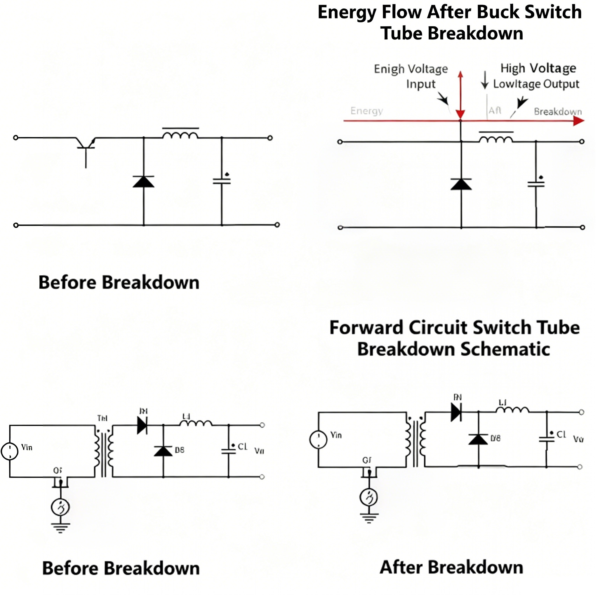
Input Bridge Rectifier and Beyond: Measure resistance across large capacitors. Low resistance indicates possible breakdown shorting in the bridge rectifier or switching transistor (MOSFET).
Switching Transistors (MOSFET/Transistor): Measure resistance between Drain/Source or Collector/Emitter to determine breakdown.
Output Stage: Measure resistance across the output capacitor to detect short circuits—test diode characteristics in reverse bias.
Check Fuses: First, inspect whether the fuse has blown. If blown, never simply replace it without identifying the root cause (e.g., a shorted switch transistor). Otherwise, the new fuse will blow again, potentially worsening the fault.
(3) Step Three: Dynamic (Power-On) Voltage/Waveform Inspection
After connecting the isolation transformer, power up cautiously.
Measure input voltage: First, verify that the input voltage is reaching the board normally.
Measure the high-voltage capacitor voltage: Verify that the rectified and filtered DC high voltage (approximately 300-400V DC for 220VAC input) is present. If this voltage is absent, the issue lies before the input fuse, NTC, or rectifier bridge.
Check the startup circuit and Vcc: Locate the Vcc pin of the main control chip.
During initial power-up, the high voltage charges the Vcc capacitor through a startup resistor.
When the Vcc voltage reaches the chip's startup threshold (e.g., 12-16V), the chip begins operation and drives the switching transistor.
Subsequently, the auxiliary winding generates an induced voltage. After rectification, this provides continuous power to the chip (typically above the startup voltage, e.g., 15-20V).
Observe the Vcc pin waveform with an oscilloscope: Check for a drop after reaching the startup voltage (hiccup mode), which typically indicates a shorted load or feedback loop failure.
Check the drive waveform:Using an oscilloscope (ensure the probe's ground clip is connected to the primary side ground!), observe the drive output pin (Gate Drive) of the main control chip or the gate (Gate) of the switching transistor.
You should observe a clean square wave pulse.
If no waveform is present, the issue may lie with the chip itself, the Vcc power supply, or the chip's enable/protection pins.
If the waveform is distorted or exhibits severe ringing, this may indicate issues with the driver circuit, transformer, or layout.
Check the secondary output:
Use a multimeter to measure whether the output voltage is near the expected value.
If the output voltage is incorrect, the problem may lie in:
Feedback loop: This is the most common problem area. Inspect the optocoupler, reference sources like the TL431, and surrounding resistors/capacitors. It is crucial to observe the feedback waveform on the optocoupler's primary side using an oscilloscope.
Output rectifier diodes: Check for breakdown or open circuits.
Output filter capacitor: Check for failure.
(4) Step Four: Common Faults and Troubleshooting Approach
|
Fault Phenomenon |
Possible Causes |
Troubleshooting Focus |
|
No output, fuse blown |
Input surge, rectifier bridge breakdown, switching tube (MOSFET) breakdown, main capacitor short circuit |
The static resistance method focuses on checking whether the rectifier bridge and MOSFET are short-circuited. |
|
No output, fuse intact |
Startup resistor open circuit, Vcc capacitor failure, main control chip damage, severe open circuit in the feedback circuit, overcurrent protection activated |
Check if the high-voltage DC is normal -> Check the startup resistor -> Check the Vcc voltage and its waveform (whether it "hiccups") -> Check the basic working conditions of the chip. |
|
Output voltage is low |
Overload, insufficient input voltage, feedback loop misalignment (e.g., TL431 voltage divider resistor value change), increased output diode voltage drop |
Check if it is normal under no-load test -> Check feedback loop components (especially voltage divider resistors) -> Check diodes and capacitors. |
|
Output voltage is high (Dangerous!) |
Open circuit in feedback loop (e.g., damaged optocoupler, cracked PCB, TL431 failure), inaccurate Vref |
Power off immediately! Focus on checking the optocoupler and the circuit around TL431. Exercise extreme caution even during no-load testing. |
|
Excessive output ripple noise |
Output filter capacitor aging/ESR increase, poor PCB layout, poor feedback loop compensation, poor reverse recovery of rectifier diode |
Observe the ripple with an oscilloscope -> Connect a good capacitor in parallel at the output end to see if it improves -> Check the ground wire layout. |
|
A "squeak" sound |
Poor dipping of transformer/inductor, unstable loop (in subharmonic oscillation), overload, voltage effect of ceramic capacitor |
Identify by sound -> Use an oscilloscope to see if there is oscillation in the waveform -> Tap the components lightly to see if the sound changes. |
5.Application Scenarios
5.1 Consumer Electronics
(1) Core Functionality
High-efficiency power conversion: Utilizes high-frequency switching technology to convert AC to stable DC, achieving conversion efficiency exceeding 85%. Some products feature nearly half the size, meeting portability and fast-charging demands.
Stable Output & Low Noise: Provides stable low-voltage DC power (e.g., 5V/12V) for electronic devices while effectively controlling ripple to prevent current interference from affecting device performance.
(2) Specific Application Scenarios
Mobile Devices
Smartphones/Laptops: Integrated power modules support fast charging technologies (e.g., fully charging a 5000mAh battery in 30 minutes) while meeting high-power demands.
Tablets/Smartwatches: Lightweight design extends battery life.
Home Appliances
TVs/Audio Systems/Air Conditioners: Achieve high-efficiency operation through switching power supplies, reducing energy consumption.
Digital Accessories
Routers/Set-Top Boxes/Security Cameras: Provides stable power support to ensure continuous device operation.
(3) Technical Advantages
Size and Weight: Modular design allows easy integration into devices without compromising portability.
Heat Dissipation: High-frequency switching technology minimizes heat generation, enhancing device stability.
Compatibility: Supports multiple input voltages to adapt to regional power grid standards.
5.2 Industrial & Communication
(1) Providing a Stable Power Supply for Industrial Equipment
Switching power supplies deliver stable power to diverse industrial equipment, ensuring reliable operation. This includes but is not limited to programmable logic controllers (PLCs), industrial robots, sensors, actuators, and controllers on automated production lines. Their high stability and reliability enable continuous operation in complex and harsh environments, enhancing production efficiency and quality.
(2) Applications in Motor Drive and Control
In industrial automation, motors serve as the critical components driving diverse mechanical equipment. Switching power supplies provide robust support for motor drive and control by delivering stable DC power. They not only ensure motor operation but also enable precise control over motor speed and power through adjustable output voltage and current, meeting varied production requirements.
(3) Role in Industrial Automation Control Systems
Industrial automation control systems require stable, reliable power to ensure regular operation. As a core component of control systems, switching power supplies deliver stable DC power, guaranteeing system functionality under diverse operating conditions. Additionally, they incorporate protective features like overload and short-circuit protection, enabling timely shutdown during anomalies to prevent fault escalation.
(4) Applications in New Energy and Energy Conservation/Environmental Protection
With the continuous advancement of new energy and energy-saving environmental protection technologies, switching power supplies are increasingly applied in these fields. For instance, in solar power generation systems, they convert the direct current generated by solar panels into stable alternating current, supplying electricity to households and businesses. Furthermore, switching power supplies are widely used in LED lighting, energy-efficient motors, and other sectors, making significant contributions to energy conservation and environmental protection.
(5) Applications in Industrial Automation Networks
Within industrial automation networks, switching power supplies deliver stable power to network equipment, ensuring reliable communication and data transmission. This equipment includes routers, switches, transmission devices, and others that require consistent power for proper operation. The high stability and reliability of switching power supplies enable continuous, stable communication and data transfer in industrial automation networks, providing robust support for automated and intelligent industrial production.
In summary, switching power supplies find extensive applications across industrial sectors. Their high efficiency, stability, and reliability make them indispensable components in industrial automation and control systems. As industrial technologies continue to advance, the application domains of switching power supplies will further expand, providing enhanced support and assurance for industrial production and development.
5.3 EV & Powertrain
Primarily divided into three key systems:
(1) On-Board Charger
This is the vehicle's built-in "slow charging" device, connecting the AC charging station (AC 220V or 380V) to the battery pack.
Function: Converts AC power from the grid into DC power required by the battery and performs intelligent battery charge management.
Working Principle: It operates as a high-power, multi-stage switching power supply system.
PFC (Power Factor Correction) Stage: First, the rectifier and PFC circuit convert AC to high-voltage DC (e.g., 400V), ensuring the current waveform and phase drawn from the grid align with the voltage. This improves power factor and reduces grid interference. This essential step resembles a PC power supply but operates at higher power levels.
DC-DC Isolation Conversion Stage: Subsequently, a high-frequency isolated DC-DC converter (often employing an LLC resonant topology) transforms the high-voltage DC output from the PFC to the voltage level required by the battery pack (e.g., 200-450V or higher) and performs precise constant current/constant voltage (CC/CV) charging control.
Technical Features:
High Power Ratings: Ranging from 3.3kW to 11kW, 22kW, and beyond.
Bidirectional Functionality Trend (V2X): Advanced OBCs employ bidirectional switching power supply topologies. They not only charge batteries with AC power (V2G) but also convert DC power from the battery back into AC power. This power can be fed back to the grid (Vehicle-to-Grid) or used for home applications (V2H). This enables the vehicle to function as a mobile energy storage unit.
(2) Low-voltage DC-DC converter
This serves as the electric vehicle's "12V power supply," replacing the generator and battery found in traditional internal combustion engine vehicles.
Function: Steps down high-voltage DC (e.g., 400V) from the battery pack to stable 12V/24V low-voltage DC, powering the vehicle's low-voltage electrical systems such as headlights, instrument panels, windows, audio systems, ECUs (Electronic Control Units), and VCU (Vehicle Control Units).
Working Principle: Typically operates as an isolated step-down switching power supply (e.g., flyback or forward type). Isolation is a mandatory safety requirement, ensuring reliable electrical separation between high-voltage and low-voltage sides (usually achieved via high-frequency transformers and optocoupler feedback) to prevent hazardous high-voltage intrusion into low-voltage systems.
Technical Features:
High Reliability: Serves as the vehicle's "lifeline." Failure renders the vehicle inoperable, causing all low-voltage systems to shut down.
Continuous Operation: Must remain active whenever the vehicle is started or in standby mode.
(3) Traction Inverter / Motor Controller
This is the "heart" of the electric vehicle's powertrain system, representing the most technologically advanced and core switching power supply application.
Function: Converts high-voltage direct current (DC) from the battery pack into precisely controllable three-phase alternating current (AC) to drive the traction motor, thereby controlling vehicle acceleration, deceleration, and speed. During regenerative braking, it functions as a rectifier, converting the three-phase AC generated by the motor (acting as a generator) back into DC to recharge the battery.
Working Principle: Essentially a high-power, three-phase DC-AC inverter. Its core is a three-phase full-bridge circuit composed of six high-power IGBT or SiC MOSFET switches. Using Pulse Width Modulation (PWM) technology, these six switches are controlled to turn on and off in an orderly sequence at extremely high frequencies (typically thousands to tens of thousands of Hz), effectively "chopping" the DC into an analog sinusoidal AC waveform.
The control chip (MCU) precisely regulates the output AC voltage and frequency by adjusting the width (duty cycle) and frequency of the PWM wave, thereby enabling precise control over the motor's torque and speed.
Technical Features:
Extremely High Power: Ranging from tens of kW to hundreds of kW, depending on the vehicle model.
Ultra-high efficiency: Every 1% efficiency gain translates to extended range. Consequently, next-generation inverters widely adopt silicon carbide (SiC) MOSFETs over traditional silicon-based IGBTs, as SiC devices offer higher switching frequencies, lower switching losses, and superior temperature tolerance.
Precision Control Algorithms: Requires deep integration with the motor to implement complex algorithms like Field-Oriented Control (FOC).
6. Maintenance & Optimization
6.1 Troubleshooting Common Issues
(1) Common Fault Analysis of Switching Power Supplies
Blown Fuse
Generally, a blown fuse indicates an internal circuit issue within the power supply.
Short Circuit: A short circuit occurs on the circuit side, causing the fuse to blow instantly.
Overload: Load current exceeds the fuse's rated current, causing prolonged heating and eventual blowout (typically occurs at approximately 1.1 times the rated current after about one hour).
Pulse Current: A momentary surge during circuit startup or power instability causes the fuse to blow.
Additionally, loose mounting screws or damaged fuses can cause tripping. Distinguish between short circuits and overloads: A short circuit directly connects live and neutral wires, bypassing appliances, creating an unimpeded current path. The massive current passing through the fuse causes its resistance to surge, generating heat that instantly melts the fuse.
Overcurrent occurs when the total power consumption of appliances exceeds the capacity, resulting in an excessive current draw. As additional appliances are turned on, the current through the fuse continuously increases. The fuse's resistance gradually rises, generating heat until it melts.
No DC voltage output or unstable voltage output
If the fuse is intact, no DC voltage is output at any level under load conditions. This situation is primarily caused by the following reasons: open circuits or short circuits within the power supply, malfunctioning overvoltage or overcurrent protection circuits, auxiliary power supply failure, non-functioning oscillator circuits, excessive power supply load, breakdown of rectifier diodes in high-frequency rectification and filtering circuits, or leakage in filter capacitors.
If the fuse is intact, no DC voltage output is present at any stage under load conditions. This situation is primarily caused by the following reasons: open circuits or short circuits within the power supply, malfunctioning overvoltage or overcurrent protection circuits, auxiliary power supply failure, inoperative oscillation circuits, excessive power supply load, breakdown of rectifier diodes in the high-frequency rectification and filtering circuit, or leakage in the filter capacitors. When measuring secondary components with a multimeter and ruling out breakdown of the high-frequency rectifier diode or load short circuit, if the output remains zero, it confirms a fault in the power supply's control circuit. If partial voltage output is present, it indicates the preceding circuit functions normally, with the fault residing in the high-frequency rectification and filtering circuit. The high-frequency filter circuit primarily consists of rectifier diodes and low-voltage filter capacitors to generate a DC output. A blown rectifier diode will cause zero output voltage, while a leaking filter capacitor may result in unstable output voltage. Static testing of corresponding components with a multimeter can identify damaged parts.
Poor Power Supply Load Capacity
Poor power supply load capacity is a common fault, typically occurring in older or long-operating power supplies. Primary causes include component aging, unstable switching transistor operation, and inadequate heat dissipation. Focus inspections should cover: - Whether the zener diode is overheating or leaking - Damage to rectifier diodes - Damage to high-voltage filter capacitors.
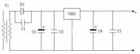
Upon inspection, the 5V DC power supply for the spectrometer's mainboard was only delivering approximately 2.3 volts. After disconnecting the load from the 5V DC power supply and powering it on again, the voltage returned to 5V. This indicated the poor load-carrying capacity of the 5V DC supply. Upon disassembling the power supply casing for inspection, since the 5V DC output was present without a load, the focus shifted to the secondary winding output rectifier circuit. Connecting a dummy load to the 5V power supply and measuring revealed a voltage of 5.2V between pins 1 and 2 of the 7805 triple regulator, while only 2.3V remained between pins 2 and 3. As shown below, this indicates the 7805 regulator had degraded performance. Replacing the 7805 regulator resolved the issue.
(2) Switching Power Supply Repair Techniques
Switching power supply repair can be conducted in two steps:
With power disconnected, perform "Observe, Smell, Ask, Measure"
Look: Open the power supply casing to check if the fuse is blown. Inspect the internal components. If scorched areas or cracked components are found on the PCB, focus on examining those components and related circuit elements.
Smell: Check for a burnt odor inside the power supply and inspect for charred components.
Ask: Inquire about the circumstances leading to the power supply failure and whether any improper operations were performed.

Measure: Before energizing, use a multimeter to measure the voltage across the high-voltage capacitor terminals. If the failure is due to the switching power supply failing to oscillate or an open switch transistor, the voltage across the high-voltage filter capacitor often remains charged at over 300 volts—exercise caution. Measure the forward and reverse resistance across the AC power cord terminals and the capacitor charging status with a multimeter. Resistance values should not be excessively low, as this may indicate an internal short circuit. The capacitor should be capable of charging and discharging. Disconnect the load and measure the resistance to ground for each output terminal group. Under normal conditions, the meter needle should oscillate as the capacitor charges and discharges, with the final reading indicating the value of the discharge resistor for that circuit.
Power-On Testing
After powering on, observe whether the power supply has blown fuses or if individual components are smoking. If so, immediately disconnect the power supply for maintenance.
Measure whether there is a 300-volt output across the high-voltage filter capacitor. If absent, focus on checking the rectifier diodes, filter capacitors, etc.
Measure whether the secondary winding of the high-frequency transformer has output. If no output is present, focus on checking whether the switching transistor is damaged, whether oscillation occurs, or whether the protection circuit has activated. If production is present, focus on inspecting the rectifier diodes, filter capacitors, and Zener diodes on each output side.
If the power supply starts briefly, then stops, it is in protection mode. Directly measure the voltage at the PWM chip's protection input pin. If the voltage exceeds the specified value, the power supply is in protection mode. Focus on identifying the cause of the protection trigger.
(3) Specific Methods for Switching Power Supply Repair
When repairing a switching power supply, first use a multimeter to check for breakdown or short circuits in power components such as the rectifier bridge, switching transistors, high-frequency power rectifier diodes, and surge-current suppression resistors. Then, verify whether the resistance at each output voltage terminal is abnormal. Replace any damaged components with new ones.
After completing these checks, if the unit still fails to operate normally after powering on, proceed to inspect the Power Factor Correction (PFC) module and Pulse Width Modulation (PWM) components. Consult relevant documentation to understand the function of each pin on the PFC and PWM modules and the essential conditions for their proper operation.
For power supplies with PFC circuits, measure the voltage across the filter capacitor. A reading of approximately 380VDC indicates the PFC module is functioning correctly. Next, verify the operational status of the PWM component. Measure the voltage at the power input terminal VC, the reference voltage output terminal VR, and the startup control terminals Vstart/Vcontrol to ensure they are within normal ranges. Power the switching power supply using a 220VAC/220VAC isolation transformer. Observe the waveform at the PWM module's CT terminal relative to ground using an oscilloscope. It should exhibit a well-defined sawtooth or triangular waveform. For example, the TL494 CT terminal displays a sawtooth waveform, while the CT terminal of the FA5310 produces a triangular wave. Verify that the waveform at the output terminal V0 is an orderly, narrow pulse signal.
In practical switch-mode power supply repair, many units employ the UC38xx series 8-pin PWM components. Most power supply failures stem from damaged startup resistors or degraded chip performance. When R breaks, the absence of VC prevents the PWM component from functioning, necessitating replacement with a resistor matching the original power rating. After increasing the PWM component's startup current, the R value can be reduced until the PWM component operates normally. While repairing a GE DR power supply with a UC3843 PWM module, no other abnormalities were detected. After connecting a 220K resistor in parallel with R(220K), the PWM module functioned normally with a stable output voltage. Occasionally, peripheral circuit failures cause the VR terminal's 5V voltage to drop to 0V, rendering the PWM component inoperative. While repairing a Kodak 8900 camera power supply, this issue occurred. Disconnecting the external circuit connected to the VR terminal restored the VR voltage from 0V to 5V, enabling the PWM component to function normally with all output voltages within specifications.
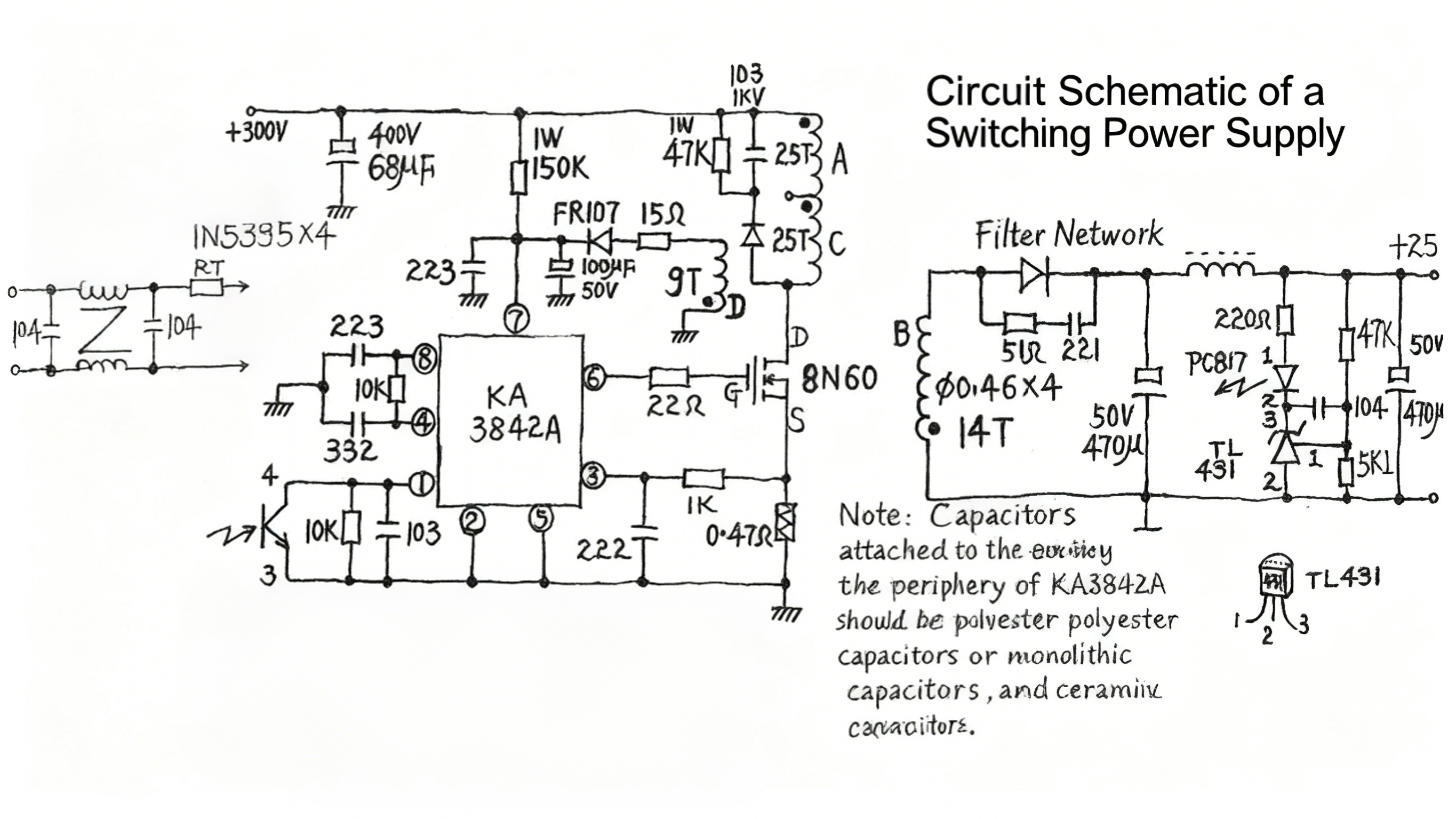
When the filter capacitor lacks approximately 380VDC voltage, it indicates the PFC circuit is not functioning correctly. Key detection pins for the PFC module include the power input pin VC, the start pin Vstart/control, the CT and RT pins, and the V0 pin. While repairing a Fujifilm 3000 camera, testing revealed no 380VDC voltage on the filter capacitor of one board. The waveforms for VC, Vstart/control, CT, RT, and V0 were all normal. However, no V0 waveform was measured at the gate (G) of the field-effect power switch transistor. Since the FA5331 (PFC) is a surface-mount component, prolonged use caused a cold solder joint between the V0 terminal and the board, preventing the V0 signal from reaching the transistor's gate. After properly soldering the V0 terminal to the board, the filter capacitor showed 380VDC voltage when measured with a multimeter. If the PFC fails to operate even when the Vstart/control terminal is at a low level, inspect the related circuits connected to its terminals and peripherals.
In summary, switching power supply circuits vary in complexity, power ratings, and output voltages. Grasping their core principles—thoroughly understanding the basic structure of switching power supplies and the characteristics of PFC and PWM modules, along with their fundamental operating conditions—and following the steps and methods outlined above while actively practicing repairs will enable rapid troubleshooting and achieve twice the result with half the effort.
6.2 Optimization Tips for Efficiency & Thermal
Optimizing the efficiency of a switching power supply is a systematic endeavor involving multiple aspects. Below are some key optimization methods:
(1) Utilize high-quality transformers
As a core component of switch-supplies, high-quality transformers reduce losses and enhance efficiency. They effectively minimize iron and copper losses, improving power conversion efficiency while extending the power supply's lifespan.
(2) Optimize Switching Component Selection
Switching components significantly impacts the efficiency of switching power supplies. Selecting switching devices such as MOSFETs with low on-resistance and high switching speed, or IGBTs with high switching speed, can substantially reduce conduction losses and switching losses.
When selecting switching components, evaluate multiple factors, including performance metrics, operating temperature, and conduction losses. Choose elements that enhance efficiency while ensuring stability and reliability.
(3) Optimize Topology Selection
Different topologies (e.g., Buck, Boost, Buck-Boost, Flyback) exhibit distinct efficiency characteristics and application scenarios. For instance, in low-voltage, high-current applications, the Buck topology is frequently chosen due to its simplicity and high efficiency.
Selecting an appropriate topology can fundamentally enhance power supply efficiency.
(4) Optimizing Switching Frequency
Increasing the switching frequency reduces the size and weight of filtering components but simultaneously increases switching losses. Therefore, it is necessary to find the optimal balance between switching losses and filtering effectiveness based on the specific application scenario.
Employing soft switching techniques (such as Zero Voltage Switching, ZVS, or Zero Current Switching, ZCS) can effectively reduce switching losses during the switching process.
(5) Precise Duty Cycle Control
The precision of duty cycle control directly impacts output voltage stability and efficiency. Employing high-precision PWM (Pulse Width Modulation) controllers () with feedback circuits (e.g., ) enables precise duty cycle adjustment. This minimizes over-regulation or under-regulation, thereby improving power supply efficiency.
(6) Utilizing low-loss magnetic materials
Core losses constitute a significant component in switching power supplies. Employing low-loss magnetic materials such as ferrite or amorphous alloys reduces core losses and enhances conversion efficiency.
Reasonably designing the magnetic circuit structure, such as using distributed windings, can also effectively reduce core losses.
(7) Incorporating intelligent control algorithms
Implementing advanced control algorithms like fuzzy logic, neural network control, and others enables dynamic adjustment of control parameters based on real-time operating conditions, achieving more precise power and higher efficiency.
For example, predictive current control technology can preemptively adjust switching states to reduce overshoot and undershoot, thereby improving power supply efficiency.
(8) Enhanced Thermal Management
Switching power supplies generates significant heat during operation. If not dissipated promptly, this heat can cause temperature rises that degrade switching device performance and lifespan, potentially leading to failures.
Therefore, effective thermal design is crucial for improving switching power supply efficiency. Specific measures include selecting high thermal conductivity materials (e.g., metals like aluminum or copper), designing optimal heat dissipation structures (e.g., adding heat sinks, employing forced air cooling fans, or implementing liquid cooling systems), and optimizing power supply layout.
6.3 Case Study
Switching power supplies utilize electronic switching devices like transistors and MOSFETs to control circuits, causing them to switch on and off continuously. By modulating the input voltage pulses through these electronic switches, voltage conversion—such as step-up or step-down—is achieved. Their advantages include a wide input voltage range, broad conversion capabilities, high efficiency, and compact size, making them widely adopted in electronic hardware. Understanding them is therefore crucial.
Grasping one or two switching power supply circuit principles can yield twice the result with half the effort, much like solving math examples.
Below are several examples of switching power supply circuits.
(1) Self-oscillating Switching Regulator
A self-oscillating switching regulator is a type of switching power supply that utilizes an intermittent oscillation circuit. Its secondary winding (including the load) section is identical to that of a single-ended flyback switching regulator.
The term "self-oscillating" here refers to a feedback process. When power is applied, the switching transistor conducts with a startup current. The collector current accumulates and grows in L1. In L2, due to the positive feedback voltage created by the transistor's base being positive and the emitter being negative, the switching transistor quickly saturates. Simultaneously, the induced voltage charges capacitor C1. The increasing voltage across C1 gradually reduces the base voltage of switch transistor VT1. When its base becomes negative, the switch transistor turns off. At this point, the rectifier diode in the secondary winding conducts, releasing the stored energy in the high-frequency transformer to the load.
When the switch transistor turns off, no induced voltage exists in L2. Capacitor C1 undergoes reverse charging, which gradually increases the base voltage of the switch transistor. This causes the switch transistor to turn on again, returning the circuit to its initial state. The circuit then repeats this oscillation cycle.
The switching transistor in a self-oscillating switching power supply performs both switching and oscillation functions, eliminating the need for manual control circuits—hence the term "self-oscillating."
(2) Push-Pull Switching Power Supply
The circuit diagram of a push-pull switching power supply is shown below.
This is a dual-ended conversion circuit that employs two switching transistors for control. Under the power of a square wave signal, the two transistors alternately turn on and off. The output is transmitted to the secondary coil, rectified, and filtered to produce the desired DC voltage. (Visually, it resembles a combination of two single-ended forward switching power supplies).
Advantages of the push-pull switching power supply include easy driving of the two switching transistors, high output power typically ranging from 100 to 500W, excellent transient response speed for output current, and superior voltage output characteristics. However, a disadvantage is that both switching transistors require high voltage ratings, with the voltage rating needing to be greater than twice the operating voltage.
7. Summary & Outlook
7.1 Recap
This article systematically introduces switching mode power supplies (SMPS) from foundational concepts, covering their definition, operating principles, common topologies, key design considerations, application scenarios, testing methods, maintenance optimization, and future trends—encompassing all aspects from theory to practice.
(1) Fundamentals and Background
Explains the fundamental concepts of SMPS and its significant advantages over linear power supplies: high efficiency, compact size, lightweight design, and wide input range. Emphasizes the critical role of SMPS in voltage conversion, energy efficiency, stability, and overload protection.
(2) Working Principles and Topologies
Detailed explanation of the five core operational steps of SMPS: rectification, switching, chopping, energy storage and conversion, filtering, and feedback regulation.
Introduces several common topologies:
Non-isolated: Buck (Step-Down), Boost (Step-Up), Buck-Boost (Converter)
Isolated: Flyback, Forward, Push-Pull, Half-Bridge/Full-Bridge, etc.
Compares the advantages, disadvantages, and application scenarios of isolated versus non-isolated SMPS.
(3) Key Design Considerations
Component Selection: Methods for selecting MOSFETs, diodes, and inductors, along with key parameters (e.g., Rds(on), Vf, DCR, inductance, etc.).
PCB Layout and Thermal Management: Emphasis on minimizing high-frequency loops, single-point grounding, and thermal design (e.g., thermal vias, heat sinks).
Control Loop and Stability: Introduces feedback loop structures, Bode plot analysis, and the importance of phase margin and gain margin.
(4) Usage and Testing
Provides SMPS selection guidelines, wiring safety precautions, load testing, and troubleshooting methods.
Highlights the critical role of oscilloscopes, multimeters, and isolation transformers in debugging.
(5) Application Scenarios
Covers three major domains: consumer electronics, industrial communications, and electric vehicles. Details the role of SMPS in various systems (e.g., OBC, DC-DC converters, traction inverters).
(6) Maintenance and Optimization
List troubleshooting methods for common faults (e.g., blown fuses, no output, abnormal output voltage).
Proposes efficiency optimization recommendations: selecting high-quality transformers, optimizing switching frequencies, employing soft-switching techniques, and utilizing intelligent control algorithms.
Case studies (e.g., self-oscillating and push-pull power supplies) enhance understanding.
7.2 Future Trends (GaN, Digital Control SMPS)
(1) Advancements in High-Frequency Technology
The rapid advancement of society undoubtedly imposes new demands on switching power supply technology. Currently, the switching frequencies of switching converters have significantly increased compared to previous eras. Simultaneously, as frequencies continue to rise, the physical size of switching converters is steadily decreasing, presenting opportunities for further refinement of switching power supply technology. However, the emergence of high-frequency switching technology will inevitably accelerate component losses within the switches and may trigger a series of associated issues.
(2) Development of Digital Technology
For traditional switching power supplies, analog signals guide the operation of control components. Today, digital control has become the predominant control method for most equipment, and switching power supplies are equally poised to become a primary application area for digital technology in the future. Currently, research into digital power supply technology has become a key focus for scientists and engineers, yielding numerous research achievements that undoubtedly play a crucial role in advancing the digitalization of switching power supply technology. In the future, digitalization will certainly become one of the hottest trends pursued by the market.
(3) Advancements in Low-Output Voltage Technology
It is widely recognized that semiconductors play a vital role in switching power supplies. The rapid advancement of semiconductor technology will directly contribute to the positive development of switching power supply technology. At present, for microprocessors and portable electronic devices, the stability of their operating voltage is critical to device functionality. Therefore, future semiconductor device converters must operate at lower voltages to ensure high-quality performance of microprocessors and electronic equipment, thereby further clarifying the direction for switch-mode power supply development.
(4) The Development of Modular Technology
Modular technology encompasses two aspects: power devices and power supply units. Through modularization, the physical size of switching power supplies can be significantly reduced. All hardware components can be integrated without compromising system reliability, enabling them to be modularly installed as chips within a single unit.
(5) Compact, integrated switching power supplies will become mainstream in modern power delivery equipment.
Miniaturization and weight reduction are particularly crucial for portable electronic devices such as mobile phones and digital cameras. Therefore, enhancing the power density and conversion efficiency of switching power supplies to achieve compactness and lightness remains an ongoing industry pursuit. High-frequency operation, soft-switching technology, and modularization are the primary technical approaches for power supply miniaturization and will become key industry focal points.
(6) Energy-saving, low-carbon, and eco-friendly products are gaining traction in the market.
Low-carbon economics has gradually become a global consensus for economic development. While adjusting its financial structure, China has elevated low-carbon and environmental protection to new heights. With the establishment of energy-saving and environmental protection targets across various sectors, green switching power supply products will see widespread adoption. This is reflected explicitly in their significant energy-saving performance and the absence of pollution to public power grids. National industrial policies will continue to favor the development of switching power supplies.