Pull Down Circuit: What It Does, How to Choose Resistor Values & Practical Design Tips
In digital circuit design, ensuring that signals not actively driven remain in a known state is critical. The pull-down circuit is one of the key techniques for achieving this goal.
Pull-Down Circuits — Definition & Purpose
What is a pull-down circuit?
A pull-down circuit is a simple configuration that connects a signal line to ground (GND) via a resistor. When no external source drives the signal, the resistor pulls the signal voltage down to a defined low level (typically 0V), ensuring the circuit has a known state when not actively driven.
What Does a Pull-Down Circuit Do?
Pull-down circuits play a vital role in electronic design by ensuring signal line stability and reliability, enhancing a system's immunity to interference. Through proper selection of resistor values and design parameters, pull-down circuits deliver outstanding performance across diverse applications. For electronic engineers, mastering the design and application of pull-down circuits is a key skill for improving system stability and reliability.
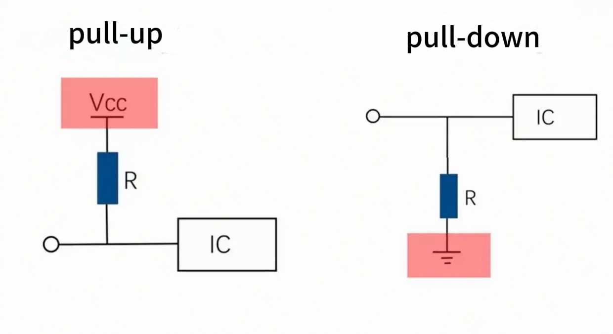
Pull-up vs Pull-down — Key Differences
Pull-up and pull-down circuits share the same objective: to provide a defined state. However, their connection methods and default states are opposite.
| Characteristics | Pull-up | Pull-down |
| Connection | Resistor connected to power supply (VCC) | Resistor connected to ground (GND) |
| Default State | High | Low Level |
| Active drive state | Must be pulled low (e.g., grounded) | Requires pulling up (e.g., to VCC) |
When to Use Pull-Down vs Pull-Up (Design Criteria)
In logic circuit design, pull-up resistors are often used to ensure bus lines like I2C or SPI remain high when not actively driven low. They are also employed for certain input devices, such as sensors and buttons, to guarantee a defined default state when not activated.
Choosing Pull-down Resistor Values
• From the perspective of power dissipation
Pull-up resistors connect to the power supply, while pull-down resistors connect to GND. When selecting resistor values, account for the power dissipation inherent to the resistor itself. For example, in a button circuit, a 10K resistor may suffice, but a 20K resistor also meets the requirement. However, the 20K resistor clearly consumes less power. In circuits requiring low standby power, strict control over pull-up and pull-down resistor values is essential. When adding pull-down resistors to signal lines, calculate the bandwidth of the first-order RC filter to prevent excessive signal attenuation and severe distortion caused by overly large R or C values.
• From the perspective of drive capability
Driving capability is closely related to the available current path. For example, in open-collector (OC) and open-drain (OD) gate circuits, an excessively large pull-down resistor prevents sufficient conduction current from being provided to the downstream circuit when the output is at a low level.
• From the signal line perspective
When adding pull-down resistors to signal lines, calculate the bandwidth of the first-order RC filter to avoid selecting R or C values that are too large. This prevents excessive signal attenuation and severe distortion.
Theory: Leakage, Logic Thresholds & RC Time Constant
• Leakage Current: Refers to the minute current present at a circuit node when not actively driven. The pull-down resistor must counteract leakage current to prevent abnormal node potential drift.
• Logic Thresholds (V_IL/V_IH): V_IL is the maximum input low level, V_IH is the minimum input high level. The pull-down resistor must ensure the node's low level is ≤ V_IL to prevent logic misinterpretation.
• RC Time Constant: Composed of the pull-down resistor (R) and total parasitic capacitance (Ctotal) (including pin and trace capacitance) on the node, it determines the signal rise time (for pull-down to High transition). Selection must align with circuit response time requirements.
Formulae & Example Calculations
• Drive Capability and Current Limitation
Microcontroller IO Port Drive Capability: For example, STM32 IO ports typically exhibit very low leakage current (μA level) in input mode. However, ensure the pull-down resistor does not cause current exceeding the IO port's maximum allowable input current (e.g., STM32F103 IO ports have an input current limit of approximately ± 25mA).
Reference Formula:
Minimum resistance Rmin =Vcc/IOH,max, where VCC is the supply voltage and Imax is the maximum allowable input current for the IO port.
Example: For VCC = 3.3V and Imax = 10mA, Rmin ≈ 330 Ω.
• Low-Level Threshold and Noise Tolerance
Ensure signal stability at low level: After pull-down, the pin voltage VOL must be below the chip's low-level threshold (e.g., VOL ≤ 0.8V in TTL circuits, typically 0.3VCC in CMOS circuits).
Noise tolerance calculation:
Maximum resistance Rmax ≤VIL,max/ILeak,max, where IIL is the maximum leakage current at the input low level (typically in the μA range).
Example: VIL,max = 0.8V, ILeak,max = 10 μA, then Rmax ≈ 80k Ω.
• Power Consumption and Leakage Current
Low-power scenarios: Higher resistance reduces power consumption (P = R × VCC ² ), but excessive resistance may increase pin susceptibility to noise interference.
Typical power consumption reference:
A 10k Ω resistor consumes approximately 1.1mW at 3.3V;
A 100k Ω resistor consumes approximately 0.11mW.
• Signal Frequency and RC Time Constant
High-Speed Signal Scenarios: Pull-down resistors form RC circuits with pin capacitance (e.g., PCB parasitic capacitance, chip input capacitance). Excessively high resistance slows signal rise times, impacting timing.
The time constant τ = R × C, typically requiring τ ≤ 10T (where T is the signal period).
Example: For a 1MHz signal (1 μs period) with capacitance C=100pF, R ≤ 10k Ω.
Typical Ranges & Why They Vary (TTL vs CMOS)
|
Resistor Value |
Typical Application Scenarios |
Characteristics |
|
1kΩ–10kΩ |
High-speed buses (SPI, USARTA), button debouncing |
Fast response, higher power consumption |
|
10kΩ-47kΩ |
General-purpose GPIO pull-down |
Balances power consumption and noise immunity |
|
100kΩ-1MΩ |
Low-power systems, battery-powered devices |
Extremely low power consumption; noise protection required |
|
Used with capacitors |
Button debouncing (10kΩ + 0.1μF), signal filtering |
Enhanced interference resistance |
• TTL vs CMOS
TTL devices: Pull-down resistors typically range from 1k Ω to 10k Ω.
CMOS devices: Pull-down resistors are typically selected between 10k Ω and 100k Ω, and can even reach the M Ω range.
• Reasons for the difference
Differing input impedances: CMOS features extremely high input impedance with minimal leakage current, allowing for higher-value resistors; TTL has lower input impedance, requiring smaller resistors to ensure sufficient drive current.
Logic threshold differences: TTL has a higher V_IL threshold (0.8V), requiring resistors to pull the potential down quickly; CMOS has an extremely low V_IL threshold (approximately 0.3VCC), offering greater tolerance for resistor values.
PCB Environment: Addressing Parasitic Parameters and Layout Effects
• Key Issue: Traces and pads on the PCB introduce parasitic capacitance (C_parasitic), potentially increasing the RC time constant and slowing level transitions. Additionally, proximity to high-noise components in the layout can cause interference.
• Adjustment Method: If parasitic capacitance is high, appropriately reduce the pull-down resistance value (e.g., from 10k Ω to 4.7k Ω ) to counteract the capacitance's impact on switching speed and ensure rapid level pull-down.
When proximity to noise sources such as power supplies or clocks is unavoidable, prioritize placing pull-down resistors between signal nodes and ground. Avoid excessively high resistance values (e.g., ≤10kΩ for high-noise/high-speed) to minimize the high-impedance path that is susceptible to noise coupling.
Long-Line Environments: Addressing Delay, Reflection, and Loss
• Key Issues: Long traces (typically >30cm or exceeding 1/20 of the signal wavelength) significantly increase propagation delay and signal reflection, while parasitic resistance/capacitance becomes more pronounced, leading to unstable signal levels.
• Adjustment Methods:
For basic signal level stabilization (not for strict impedance matching): Use lower resistor values than in short-cable scenarios (e.g., reduce TTL from 1kΩ–10kΩ to 470Ω–4.7kΩ) to accelerate level response and prevent logic misjudgment caused by delay.
For high-speed transmission line impedance matching: Prioritize matching the transmission line's characteristic impedance (e.g., 50Ω/75Ω). Selecting pull-down resistors close to the characteristic impedance (e.g., 47Ω/51Ω) serves as a form of parallel termination. Note that this approach incurs high power consumption and high drive current requirements. Alternatively, consider series termination resistors where applicable.
Noise Environments: Enhancing Interference Resistance
• Key Issue: Electromagnetic interference (EMI), ground bounce noise, etc., cause signal node potential fluctuations. Excessively high pull-down resistor values weaken interference resistance, potentially triggering erroneous logic.
• Adjustment Method: Reduce pull-down resistance (e.g., from 10k Ω– 100k Ω to 4.7k Ω– 22k Ω for CMOS) to lower node input impedance and minimize noise coupling energy.
For extremely high noise levels, parallel a 100pF to 1nF filter capacitor with the pull-down resistor to form an RC filter network, further suppressing high-frequency noise. However, avoid excessive impact on switching speed.
unikeyic's Exclusive Perspective: Trade-offs Between Low Power Consumption and High-Frequency Device Performance
When optimizing BOMs for clients, we frequently encounter this trade-off.
• Battery-powered products: We prioritize low power consumption. We use 100k Ω or larger pull-down resistors, even if this sacrifices some edge speed, because the core requirement is long battery life.
• High-speed pulse or communication interfaces (e.g., SPI, digital sensor interrupt lines): We prioritize signal integrity. Resistors ranging from 1kΩ to 4.7kΩ are used to ensure fast response and clean waveforms.
There is no "one-size-fits-all" value; the optimal choice depends on the product's primary performance metrics.
How to Tell if a Resistor is Pull-up or Pull-down
Schematic/PCB/Net-Name clues
• If one end connects to a signal line and the other to VCC or a power network, it's a pull-up.
• If the other end connects to GND or a ground network, it is pull-down.
Practical lab methods(multimeter/oscilloscope)
• For physical circuits without schematics, determine in two steps: Step 1: Measure idle node voltage. Disconnect all loads except the power supply to leave the signal node idle. Use the multimeter DC voltage setting to measure node potential--Close to Vcc: Pull-up resistor (pulls node high), Close to GND: Pull-down resistor (pulls node low)
• Second step: Verify resistor connections. With the power off, use the multimeter resistance mode: - Connect one probe to the resistor pin and the other to GND. If resistance is close to the resistor's nominal value, it is a pull-down resistor. Connect the other probe to Vcc. If resistance is close to the nominal value, it is a pull-up resistor. When using an oscilloscope, A pull-up resistor corresponds to a waveform stable at a high level during the idle state. A pull-down resistor corresponds to a waveform stable at a low level during the idle state.
MCU conventions & internal pull usage
• Pull-up/pull-down resistors on MCU boards are categorized as internal or external, with fixed identification rules: External resistors can be determined using the methods described earlier; internal resistors require checking the MCU model and pin configuration.
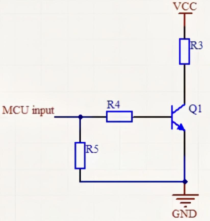
• Common conventions include the default internal pull-up resistors on Port P1 of the 51 microcontroller. For ARM-based MCUs like STM32, GPIO pins can be configured via registers as "Pull-Up Input (PU)" or "Pull-Down Input (PD)", explicitly documented in the configuration manual. In hardware design, external pull-up/pull-down resistors are commonly paired with pushbutton circuits: - Pushbuttons connected to an MCU pin at one end and GND at the other require pull-up resistors. - Pushbuttons connected to an MCU pin at one end and Vcc at the other require pull-down resistors. This represents a typical design convention for MCU boards.
Typical Applications & Wiring Examples
Buttons & Switches (schematics)
Button interfaces represent the most fundamental application of pull-up/pull-down resistors, primarily preventing unintended activation due to floating pins.
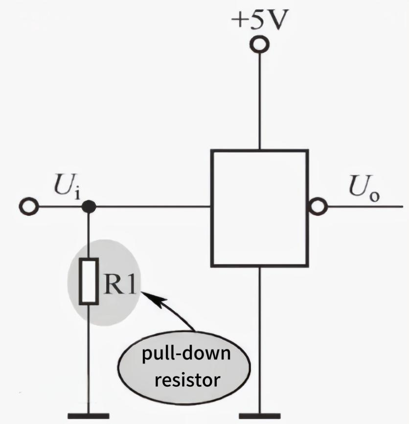
• Pull-up Wiring: One end of the button connects to the MCU pin, the other to GND. A pull-up resistor is connected between the MCU pin and Vcc. When not pressed, the resistor pulls the pin to Vcc (high level). When pressed, the pin grounds via the button (low level), triggering the circuit response.
• Pull-down configuration: One end of the button connects to the MCU pin, the other to Vcc. A pull-down resistor is connected between the MCU pin and GND. When not pressed, the pin is pulled to GND (low level); when pressed, it connects to Vcc (high level). In practical designs, the pull-up configuration is more commonly used, as it can directly utilize the MCU's built-in pull-up resistor to reduce external components.
I²C & Open-Drain buses (why pull-ups are used)
Open-drain buses like I²C typically use pull-up resistors to enable multiple devices to "wire-and" functionality. If pull-down resistors are mistakenly used, the bus will be permanently pulled low, preventing the necessary high-level signals from being generated and causing complete communication failure.
Sensor Front-Ends & ADC Inputs
For certain digital output sensors or configuration pins, pull-down resistors may be used to ensure they maintain a default low state or specific mode when not actively driven. At ADC input front-ends, a high-value pull-down resistor can serve as a weak hold to prevent noise introduced by floating inputs, but its loading effect on the signal source must be considered.
TTL Specifics (lower pull-down values sometimes required)
TTL logic inputs exhibit strong pull-down current absorption capability at low levels but weaker drive (source current) capability at high levels. To ensure reliable low levels, relatively low-value pull-down resistors (e.g., 1k Ω to 4.7k Ω ) may sometimes be required. These provide sufficient current to overcome partial leakage from internal transistors, thereby stably pulling the voltage below the effective threshold..
Maintenance & Troubleshooting
A pull-down circuit connects a resistor between the GPIO pin and ground (GND). This ensures the pin is stably pulled to a low level (0V) when the button is not pressed or the signal line is floating. This prevents false triggering caused by electromagnetic interference or internal pin instability.
Common faults & root causes
Floating Input
• Symptom: Uncertain pin level, randomly read as high or low.
False Triggering
• Symptom: System incorrectly detects input when no button is pressed.
• Cause: Pull-down resistor value is too high (e.g., >1M Ω ), resulting in weak noise immunity; external interference easily alters pin levels;
Moisture or contamination on the circuit board is causing minor leakage; Signal wires are excessively long and unshielded, acting as antennas to introduce noise.
Button bounce
• Symptom: A single physical button press triggers multiple rapid level transitions (fluctuations between high and low), leading to the MCU detecting false triggers.
Debounce: HW + SW strategies
Hardware Debouncing
• RC Filtering: Connect a 100 Ω resistor in series between the button and GPIO pin, and a 0.1µF capacitor in parallel between the GPIO pin and ground. The capacitor's charging/discharging absorbs glitch noise and smooths edges.
• Schmitt Trigger: Use ICs or MCU pins with Schmitt trigger inputs. Their hysteresis characteristics effectively suppress edge noise from signal jitter, providing clean level transitions.
Software Debouncing
• Delay Method: After the first detected level change, delay for 10-50ms (to avoid the jitter period) before reading the pin state again for confirmation.
• State detection method: Continuously scan the pin, only considering the key state as validly changed when the same state is read consecutively multiple times (e.g., 5 times). This method is more efficient.
Troubleshooting checklist
• Basic checks: Verify correct and stable connections between the power supply (VCC) and the ground (GND).
Visually inspect pull-down resistor solder joints for integrity and verify resistance matches design (typically 10kΩ ).
• Static voltage measurement: Use the DC voltage setting on a multimeter.
When the button is not pressed: Measure the voltage between the GPIO pin and ground. It should be a stable low level (close to 0V). If the voltage drifts or is unstable, check the pull-down resistor or inspect for cold solder joints or contamination.
When the button is pressed, the pin voltage should stabilize at a high level (close to VCC). If the voltage is too low, check the pull-up resistor (if present) or whether the button contact resistance is too high.
• Dynamic Waveform Capture:
Connect an oscilloscope probe to the GPIO pin under test.
Set the trigger mode to edge triggering.
Observe jitter: Operate the button normally and observe whether the rising/falling edges of the waveform are clean. If dense glitches are visible, this indicates jitter.
Verify Debouncing Effect: After implementing hardware (RC) or software debouncing measures, capture the waveform again. Clear, clean level transition edges should be visible.
• Software Logic Verification:
Set debug breakpoints or print statements in the code to verify that the pin states read by the MCU match the physical operations. Additionally, check whether the software debounce logic executes correctly.
Prototype to Production and BOM Recommendations
Optimizing the BOM (Bill of Materials) is critical during the transition from prototype to production, especially for pull-down circuit design.
Rapid Prototyping: Advantages and Disadvantages of Using MCU Internal Pull-Downs
During prototyping, leveraging the MCU's internal pull-down resistors enables rapid circuit implementation, saving external components, reducing costs, and simplifying layout. However, internal pull-downs typically suffer from low precision, limited drive capability, and poor temperature stability, potentially causing signal noise or false triggering. This poses higher risks in high-speed or high-reliability applications.
Production: resistor arrays, alternates & EMC
For mass production, replacing internal pull-downs with external SMD resistor arrays is recommended to enhance signal integrity, reliability, and consistency. Simultaneously, incorporate alternate part numbers (e.g., resistors in different packages) into the BOM to mitigate supply chain volatility. Regarding ESD and EMC, external resistors aid in impedance matching and filtering to reduce electromagnetic interference. Combining this with optimized PCB layout (e.g., short traces and ground planes) is advised to pass compliance testing.
Unikeyic Exclusive Insights: Balancing Trade-offs in BOM/Supply Chain
• The core trade-off in BOM and supply chain management is the combined benefit of "unit cost + assembly cost": When the number of pull-up/pull-down resistors on a PCB reaches ≥ 4, resistor networks offer greater cost advantages than individual resistors. For example, an 8-element resistor network costs approximately 60% of the procurement cost for eight individual resistors, and requires only one placement point — reducing placement costs by 87.5% compared to 8 individual resistors. This is particularly suitable for mass-production scenarios with monthly output ≥ 1000 pcs.
Summary & Practical Takeaways
Quick Decision Flow Cheatsheet
|
Core Scenarios |
Key Decision Points/Process |
Core Basis/Considerations |
|
Selecting Pull-Down Resistors |
Determine device type (TTL/CMOS); Specify requirements (low power/high frequency); Calculate Rmin/Rmax; Refer to empirical values |
TTL: 1k-10kΩ, CMOS: 10k-100kΩ; Low power: 100k+Ω, High frequency: 1k-4.7kΩ; Formula: Rmin = Vcc/Imax, Rmax = (Vcc - Vol)/Iil |
|
Pull-up/Pull-down Differentiation |
Schematic: Check connection to Vcc (pull-up)/GND (pull-down); Physical: Measure idle voltage (near Vcc/near GND); 3. MCU board: Refer to the manual (PU/PD) or button configuration |
Markings: PU = Pull-up, PD = Pull-down; Verify continuity by measuring resistance during power-off |
|
Troubleshooting |
Floating input: Check for missing components/excessive resistance; False Triggering: Measure voltage, adjust resistor value/check for cold solder joints; Jitter: Inspect waveform with oscilloscope, add RC circuit + software anti-jitter |
If idle voltage > 0.5V, reduce resistance value; If jitter exceeds 20ms, optimize RC |
|
Environmental Adaptation Adjustments |
High PCB parasitic capacitance: Reduce resistance (e.g., 10k → 4.7kΩ); Long cables: Match impedance (e.g., 50Ω) or reduce resistance; High noise: 4.7k-22kΩ resistor + 100pF capacitor |
High-frequency requirement: τ=R×C ≤ 10T (T=signal period) |
|
Prototype to production trade-offs |
Prototype: Prioritize MCU-integrated solutions (low-cost rapid validation); Production: ≥4 units—select SMD array, prepare 2 suppliers ; Cost: ≥1k monthly production volume and ≥4 components use resistor networks |
On-chip components are unsupported for high frequency/heavy load; High humidity: Select moisture-proof ≥RH60 |
Recommended Starting Values by Scenario
|
Application Scenarios |
Recommended Starting Values |
|
Button (key interface) |
10kΩ |
|
Low-power scenarios (e.g., IoT sensors, battery-powered devices) |
100kΩ |
|
TTL logic circuits |
4.7kΩ |
|
Long-line scenarios (length > 30cm or non-high-speed signals) |
4.7kΩ (General-purpose) / 51Ω (High-speed impedance matching) |
Related reading
ESD Suppressors Explained: Types, Applications, and Benefits