What Is a Charge-Coupled Device (CCD)? The Guide to the Technology Powering Modern Imaging
Charge-coupled devices (CCDs) are the unsung heroes of the digital imaging revolution. From capturing the first images of distant galaxies to enabling high-resolution medical diagnostics, CCDs have shaped how we see and analyze the world. Invented in 1969 by George E. Smith and Willard Boyle at Bell Labs, CCDs transformed light into electronic signals with unprecedented accuracy. This article explores the intricate workings of CCDs, their advantages over competing technologies like CMOS, and their vast applications—spanning astronomy, medical imaging, industrial systems, and even biomass combustion analysis. By delving into terms like dynamic range, noise ratio, charge transfer efficiency, and silicon substrate, we uncover why CCDs remain indispensable in precision-driven fields.
The Birth and Evolution of CCD Technology
The story of CCDs begins at Bell Laboratories, where researchers sought a way to improve memory storage for computers. Instead, George E. Smith and Willard Boyle stumbled upon a method to capture light electronically. Their invention relied on a silicon surface layered with a metal-oxide-semiconductor (MOS) structure, which could trap electrons generated by incoming photons. Early CCDs faced challenges like dark current (unwanted charges from heat) and readout noise, but innovations such as liquid nitrogen cooling and pixel binning soon mitigated these issues.
By the 1980s, CCDs became the gold standard for digital imaging, powering the first digital cameras and revolutionizing astronomy applications. The Hubble Space Telescope, for instance, used CCDs to capture faint starlight over long exposure times, thanks to their high dynamic range and low noise ratio. Meanwhile, medical imaging systems adopted CCD-based detectors for X-rays and storage phosphor imaging, providing clearer diagnostics.
Anatomy of a CCD: Breaking Down the Components
A CCD is a marvel of semiconductor engineering. Let’s dissect its core parts:
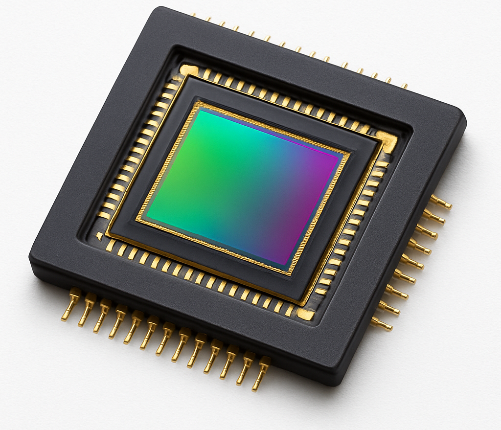
1.Silicon Substrate and MOS StructureThe foundation of a CCD is a silicon wafer coated with a photosensitive layer. When photons hit the silicon surface, they create charge electrons in the depletion region—a zone where electric fields guide charges toward gate electrodes.
2.Gate Electrodes and Charge TransferMade of polysilicon gates, these electrodes control the movement of charges. By applying alternating voltages, charges shift across adjacent pixels in a process called charge shifting. This transfer occurs through parallel shifts (vertical movement) and serial shifts (horizontal movement), directed by an array of gating electrodes.
3.Output Node and Signal ConversionCharges funnel to an output amplifier, which converts them into an analog voltage signal. This stage is prone to readout amplifier noise, but advanced designs like frame-transfer CCDs isolate imaging and storage areas to minimize interference.
4.Peripheral Components
● Dark charge level: Managed via cooling to reduce thermal noise.
● Photon statistical analysis: Ensures accurate measurement of photon flux in low-light scenarios.
● Capacitance of pixels: Affects the signal-to-noise ratio, critical for scientific measurement applications.
How CCDs Work: A Step-by-Step Journey from Light to Data
The magic of CCDs lies in three stages: charge accumulation, charge transfer, and signal readout.
1. Charge Accumulation: Capturing Photons
When light strikes the silicon substrate, photons penetrate the photoactive regions, generating electron-hole pairs. The intensity of incident light determines the number of electrons stored in potential wells beneath the gate electrodes. This step is highly sensitive to light intensity and wavelength of light, enabling CCDs to operate across a broad spectral range, from ultraviolet to infrared.
Key Factors Influencing Accumulation
● Exposure time: Longer exposures capture more photons but risk dark current buildup.
● Pixel size: Smaller pixels enhance spatial resolution but reduce light-gathering capacity.
● Absence of light: Managed by shielding the CCD or using dark charge level calibration.
2. Charge Transfer: Moving Electrons with Precision
Once charges accumulate, they must travel to the output node without loss. This is achieved through charge transfer efficiency, a metric defining how well electrons move between adjacent pixels.
● Parallel Shift Registers: Move charges row-by-row using alternate electrodes.
● Serial Shift Registers: Guide charges column-by-column toward the amplifier.
● Charge Distribution Pattern: Ensures minimal distortion during transfer, vital for high-quality images.
Innovations like two-dimensional arrays and full-frame devices optimize this process, especially in scientific applications requiring minimal noise.
3. Signal Readout: From Analog to Digital
At the output node, charges convert to a voltage signal. This stage introduces readout noise, but techniques like correlated double sampling (CDS) mitigate this. The analog signal then passes through a digital signal processing pipeline, where it’s amplified, digitized (often to 12-bit resolution), and formatted into a 2D image array.
Challenges in Readout
● Thermal noise: Reduced via liquid nitrogen cooling in high-end systems.
● Statistical noise: Addressed through pixel binning (combining multiple pixels) to boost signal strength.
Why CCDs Reign Supreme in Precision Imaging
CCDs dominate applications where accuracy trumps speed. Here’s why:
● Unmatched Dynamic Range: CCDs handle extreme variations in light intensity, preserving details in both shadows and highlights. This is crucial for astronomy applications imaging faint nebulae and bright stars in the same frame.
● Low Noise Architecture: Unlike CMOS sensors, CCDs centralize signal readout via a single output amplifier, minimizing readout amplifier noise. Combined with dark current suppression techniques, this results in cleaner images for medical imaging and scientific research.
● Superior Spatial Resolution: High-density two-dimensional arrays and small pixel size enable CCDs to resolve fine details. For example, CCD-based detectors in microscopes capture cellular structures with nanometer precision.
● Broad Spectral Sensitivity: From ultraviolet (blue components) to near-infrared, CCDs adapt to diverse imaging systems, including flame image acquisition for analyzing combustion processes.
Applications of CCD Technology: Beyond the Obvious
CCDs are not just for cameras—they’re everywhere precision matters.
1. Astronomy and Space Exploration
CCDs revolutionized astronomy by replacing photographic plates. The Hubble Space Telescope’s CCDs captured iconic images like the Pillars of Creation, leveraging their low noise ratio and photon statistical accuracy. Modern telescopes use CCD imagers with 12-bit resolution to map dark matter and exoplanets.
2. Medical Imaging
● X-ray Systems: CCDs convert X-ray photons into visible light, aiding in storage phosphor imaging for dental and chest scans.
● Endoscopy: Miniaturized CCD image sensors provide real-time visuals during surgeries.
3. Industrial and Scientific Systems
● Flame Image Acquisition: CCDs analyze biomass combustion flames, measuring temperature and photon flux to optimize energy output.
● Bar Code Readers: Linear CCD arrays scan codes rapidly, even in low-light conditions.
● Machine Vision: CCD cameras inspect manufacturing defects with micron-level accuracy.
4. Niche and Emerging Uses
● Art Restoration: CCDs detect hidden layers in paintings via multispectral imaging.
● Quantum Research: CCDs track single photons in quantum optics experiments.
CCD vs. CMOS: A Detailed Comparison
While CMOS sensors dominate consumer markets, CCDs excel in specialized niches.
| Parameter | CCD | CMOS |
|---|---|---|
|
Readout Noise |
Lower due to centralized amplification |
Higher due to per-pixel amplifiers |
|
Power Consumption |
Higher (requires external circuitry) |
Lower (integrated transistors) |
|
Speed |
Slower (sequential readout) |
Faster (parallel readout) |
|
Dynamic Range |
Wider (ideal for low-light) |
Narrower |
|
Cost |
Higher (complex manufacturing) |
Lower (standard semiconductor processes) |
Why Choose CCDs Today?
● Scientific applications: Where signal-to-noise ratios are critical.
● Legacy systems: Many industrial imaging setups still rely on CCDs.
● High dynamic range: Essential for astronomy and biomass combustion analysis.
Innovations Driving CCD Technology Forward
CCDs aren’t stagnant—they’re evolving to meet modern demands.
1.Hybrid DetectorsCombining CCDs with digital signal processing chips enhances real-time image analysis. For example, principal component analysis algorithms reduce noise in flame region imaging.
2.Back-Illuminated CCDsBy thinning the silicon substrate, these CCDs achieve higher quantum efficiency, ideal for photon flux measurement in low-light scenarios.
3.Cooling AdvancementsThermoelectric coolers replace liquid nitrogen in portable systems, making CCDs viable for field applications like environmental monitoring.
4.3D ImagingFrame-transfer CCDs with horizontal direction shift capabilities enable 3D volumetric imaging in medical scans.
The Future of CCDs: Adapting to a CMOS-Dominated World
While CMOS sensors dominate smartphones and action cameras, CCDs will persist in areas demanding uncompromised quality. Researchers like Nobukazu Teranishi (pioneer of the pinned photodiode) continue refining CCD architectures. Emerging trends include:
● Quantum CCDs: Leveraging charge distribution patterns for quantum computing interfaces.
● AI-Enhanced Imaging: Pairing CCDs with machine learning to automate scientific measurement applications.
● Space-Grade CCDs: Radiation-hardened designs for missions to Mars and beyond.
Conclusion: The Enduring Legacy of CCD Technology
From their serendipitous invention at Bell Labs to their role in cutting-edge research, charge-coupled devices have proven their worth as a cornerstone of imaging technology. Their ability to deliver high-quality images with low noise ratios, broad spectral range, and excellent spatial resolution ensures they remain irreplaceable in medical imaging, astronomy, and industrial applications. As innovations like principal component analysis and back-illuminated designs push the boundaries of what’s possible, CCDs will continue illuminating the unseen—one meticulously transferred charge at a time.
Whether analyzing biomass combustion flames or capturing the ethereal glow of distant galaxies, CCDs remind us that sometimes, the oldest technologies are the ones that shine brightest.