The Diode Clamp: Shifting Signals and Protecting Circuits
In the intricate world of electronic signal conditioning, few circuits offer the elegant simplicity and fundamental utility of the diode clamp, also known as a clamp circuit. This unassuming combination of a diode, a capacitor, and often a resistor performs a critical task: it shifts the entire DC level (the average voltage) of an alternating current (AC) signal up or down without altering the signal's shape or amplitude. Its ability to "clamp" a specific point of the waveform (typically a peak) to a defined reference voltage makes it indispensable across diverse applications, from vintage television circuits to modern precision instrumentation and robust actual input protection schemes.
The Core Principle: Capacitive Coupling and Diode Steering
The magic of the clamper lies in the interplay between its key electronic components:
1.The Capacitor (C): This component acts as the heart of the level-shifting mechanism. Placed in series with the input signal, it blocks any DC component present in the input while allowing the AC variations to pass through. Crucially, it charges or discharges during specific phases of the input cycle to establish a new DC bias voltage point. The capacitor value is chosen such that its time constant (τ = R * C, where R is the load or an explicit resistor) is significantly larger than the period of the input signal. This ensures the capacitor holds its charge relatively constant over many cycles, providing a stable DC offset.
2.The Diode (D): Acting as a voltage-controlled switch, the diode determines which part of the waveform gets clamped and the direction of the shift. It conducts heavily when forward-biased (anode voltage > cathode voltage by its forward voltage drop, Vf) and blocks current rating when reverse-biased. Its orientation dictates whether the positive peaks or negative peaks are pulled towards the reference voltage.
3.The Reference Voltage (Vref): This is the voltage level to which the chosen peak (positive or negative) is "clamped." It can be ground (0V), a positive supply voltage (V+), a negative supply voltage (V-), or any other stable DC voltage.
4.The Resistor (R) or Load: A resistor (explicit or representing the circuit's load impedance) provides a discharge path for the capacitor when the diode is not conducting. Its value, in conjunction with the capacitor, sets the time constant and influences how well the circuit maintains the clamp voltage, especially at lower frequencies.
Operational Mechanics: The Negative Clamper
Consider the most common configuration: the Negative Clamper (or Positive Peak Clamper to Ground). Here, the diode's anode is connected to the junction of the capacitor and the load resistor, while its cathode is connected to the reference voltage (usually ground).
1.Initial State (First Negative Half-Cycle): Assume the input signal starts at 0V and swings negative. The diode becomes forward-biased (anode is pulled negative relative to the grounded cathode). Current flows through the diode, charging the capacitor. The capacitor charges to approximately the peak negative voltage (Vp-) of the input voltage minus the diode's forward voltage drop (Vf). The polarity of this charge is positive on the diode side and negative on the input side. The output voltage at the cathode/anode junction is clamped near ground (0V + Vf) during this phase.
2.Following Positive Half-Cycle: The input signal now swings positive. The diode becomes reverse-biased (cathode at ~0V, anode trying to go positive). No current flows through the diode. The capacitor, now charged to Vp- (approx.), acts like a battery in series with the input signal. The output voltage is the sum of the input voltage and the capacitor voltage: Vout = Vin + Vcap. Since Vcap is negative (approx. -Vp-), when Vin reaches its positive peak (+Vp+), Vout = +Vp+ + (-Vp-) = +Vp+ - Vp-. If the signal is symmetric (Vp+ = Vp- = Vp), Vout peaks at approximately 0V. Effectively, the entire waveform has been shifted downwards by Vp volts. The positive peaks are now clamped near 0V (actually 0V + Vf). The series resistor R slowly discharges the capacitor during this phase, but if RC >> signal period, the discharge is minimal, maintaining the clamp.
3.Steady State: Subsequent cycles reinforce this behavior. The diode conducts briefly near the negative peak, replenishing any charge lost by the capacitor through R during the rest of the cycle. The output waveform retains the exact AC shape of the input but rides on a negative DC level, with its positive peaks firmly "clamped" close to the reference voltage (ground).
The Positive Clamper: Shifting Upwards
Reversing the diode orientation creates a Positive Clamper (or Negative Peak Clamper to Ground). The cathode connects to the capacitor/load junction, and the anode connects to Vref (ground).
1.Initial State (First Positive Half-Cycle): The diode is forward-biased during the positive input swing. Current flows, charging the capacitor to approximately the input's positive peak voltage (Vp+) minus Vf. The polarity is negative on the diode side, positive on the input side. Output is clamped near ground (0V - Vf).
2.Following Negative Half-Cycle: Diode is reverse-biased. Output voltage is Vout = Vin - Vcap. Since Vcap is positive (approx. +Vp+), when Vin swings to its negative peak (-Vp-), Vout = -Vp- - (+Vp+) = -Vp- - Vp+. For symmetric signals, this is approximately -2Vp. The entire waveform is shifted upwards by Vp volts. The negative peaks are clamped near ground (0V - Vf).
3.Steady State: Diode conducts briefly near the positive peak to maintain the capacitor charge. Output waveform has original AC shape on a positive DC level.
Biased Clampers: Targeting Specific Levels
Clampers are not limited to ground. By connecting the diode's reference terminal (cathode for negative clamp, anode for positive clamp) to a DC voltage source (Vbias) instead of ground, the clamping level is shifted accordingly.
● Biased Negative Clamper: Diode cathode to +Vbias. Positive peaks are clamped to +Vbias + Vf. The entire signal shifts down relative to its original position but rides on a DC level determined by Vbias and the signal swing.
● Biased Positive Clamper: Diode anode to -Vbias. Negative peaks are clamped to -Vbias - Vf. The entire signal shifts up relative to its original position.
Design Considerations and Practical Nuances
While conceptually simple, practical implementation requires attention to detail:
Diode Characteristics:
Forward Voltage Drop (Vf): Silicon diodes (0.7V) or Schottky diodes (0.3V) are common. Vf determines how close the clamped peak gets to the ideal reference voltage (Vref). For precision clamping, op-amp-based "precision clampers" or "ideal diode" clamping circuits are used.
Reverse Recovery Time: For high-frequency signals, fast recovery diodes are essential to prevent distortion during the clamping transition.
Reverse Breakdown Voltage (Vbr): Must exceed the maximum reverse voltage seen across the diode.
Leakage Current: Can cause a gradual drift in the DC level over time, especially critical for very low-frequency signals or high-impedance loads.
Capacitor Selection:
Value: Must be large enough so that RC >> T (signal period). This minimizes "tilt" or "sag" on the output waveform during the non-conducting half-cycle. Larger C reduces tilt but increases physical size and cost. C = (T * Load Resistance) / (k * Desired % Tilt) is a common starting point (k ~ 5-10).
Type: Electrolytics are common for low-frequency, high-value needs. Ceramic or film capacitors are preferred for higher frequencies or where low leakage is critical. Voltage rating must exceed the maximum voltage across it.
Resistor (R) Selection:
Value: Sets the discharge time constant with C. Must be large enough to maintain the charge (RC >> T) but small enough to allow sufficient charging excess current through the diode during its conducting phase without excessive voltage drop. Too large an R increases susceptibility to leakage currents; too small causes excessive tilt.
Power Rating: Must dissipate the power (I²R or V²/R) during discharge without overheating.
Source and Load Impedance:
The effective source impedance feeding the clamper and the load impedance connected to its output influence the actual RC time constant and the charging/discharging behavior. Output loading can significantly affect performance if not accounted for.
Ubiquitous Applications: From Analog to Digital
The diode clamp's versatility ensures its presence in numerous electronic domains:
1.Signal Level Shifting: The fundamental purpose. Used in:
Analog Video Processing (Historically Vital): Clamping the sync pulses in television signals to a fixed level (e.g., "black level" clamping) was crucial for stable picture reproduction. Modern systems often use active circuits, but the principle remains.
AC Coupled Amplifier Stages: Restoring the DC component of a signal after it has passed through a coupling capacitor, bringing it within the input range of the next stage.
Data Acquisition Systems: Shifting sensor outputs (which might swing negative or have an offset) to match the 0V to Vref input range of an Analog-to-Digital Converter (ADC).
Communications Receivers: Shifting modulated signals for optimal demodulation.
2.Input Protection:
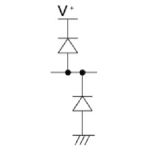
Voltage Clamping (ESD/Transient Suppression): While dedicated Transient Voltage Suppression (TVS) diodes are optimized for this, simple diode clamps are fundamental building blocks. A common configuration uses two diodes: one cathode to Vcc, anode to input; the other anode to Gnd, cathode to input. This clamps input excursions to approximately Vcc + Vf and Gnd - Vf, protecting sensitive inputs (like CMOS logic gates or op-amp inputs) from electrostatic discharge (ESD) or voltage transients exceeding the supply rails. This is arguably one of the most widespread uses today.
3.Waveform Generation: Can be used creatively with other electronic circuits to modify waveforms, such as creating square waves from sine waves or adding DC restoration to complex waveforms.
4.DC Restoration: Similar to level shifting, specifically ensuring a particular part of the signal (like the baseline or a reference level) is fixed at a known DC voltage, critical for accurate measurement or display.
Limitations and Evolution
The simple diode clamp has limitations:
● Diode Vf Drop: Prevents perfect clamping to Vref.
● Tilt/Sag: Due to capacitor discharge during the non-conducting phase, especially noticeable at low frequencies or with small capacitors.
● Loading Effects: Output load can distort the waveform.
● Current Limit Handling: Basic clampers aren't designed for high power.
To overcome these, especially the Vf limitation and tilt, designers use:
● Precision Clampers / Ideal Diode Circuit Structure: Utilize operational amplifiers to create virtual grounds or near-ideal diode behavior, effectively eliminating Vf and providing very low output impedance.
● Active Clamping: Using bipolar transistors or op-amps controlled by the clamping reference for faster, more precise control.
The diode clamp stands as a testament to the power supplies of simple yet profound electronic principles. By leveraging the unidirectional conduction of a diode and the charge storage of a capacitor, it performs the essential function of DC level shifting with remarkable fidelity to the original signal's shape. From its historical role in stabilizing television pictures to its critical modern function in protecting sensitive integrated circuits from electrical overstress and conditioning signals for digital conversion, the clamper circuit remains a vital tool in the electronics engineer's toolbox. Its elegance lies in its ability to achieve a complex task – manipulating the DC axis of a signal – through such fundamentally straightforward means. Understanding its operation, design trade-offs, and diverse applications is foundational knowledge for anyone navigating the world of analog and mixed-signal electronics. While active circuits offer higher precision, the basic diode clamp continues to offer an unbeatable combination of simplicity, robustness, and effectiveness for countless applications.