How Does a Flip Flop Work?
In practical digital systems, a large number of basic storage element are often involved, and these frequently need to operate synchronously. To achieve this clock synchronization, a clock pulse (CLK) is introduced as a control signal into each storage unit circuit. The electronic circuit is "triggered" and activated only when the CLK arrives, altering the output types based on the input signal. This type of storage unit circuit, which operates upon the triggering of the clock signal, is known as a Flip Flop, distinguishing it from a output latch, which does not have clock signal control.
Core Characteristics of Flip-Flops
● Bistability: Conventional flip-flops possess two stable states (Q=1 or Q=0), which are maintained by positive feedback within the circuit.
● Clock Control: State updates are typically triggered by a clock signal (CLK), and can be categorized into level-triggered and edge-triggered methods.
● Flip-flop Input Dependence: The output alternates is determined by the current input (such as edge-triggered D flip-flop, J/K, S/R, etc.) along with the current state.
Basic Structure of Flip-Flops
Conventional flip-flops are typically an improved version of output latches, designed to address the "transparency" issue of output latches, wherein the input directly influences the output alternates for an extended period. This is achieved by introducing a clock event.
Common structures include:
1.Master-Slave Structure: Consists of two latches in series, where the master output latch locks the control input during the high clock level, and the slave latch outputs on the falling edge of the atomic clock.
2.Edge-Triggered Structure: Utilizes gating circuits to sample the input only at the instant of the rising or falling edge of the current clock cycle.
Operation of a Flip-Flop (Using an Edge-Triggered D Flip-Flop as an Example)
Before the Clock Edge Arrives:
● The input signal D is transmitted through combinational logic to the interior of the basic flip-flop, but the output Q toggle remains unchanged.
● Setup Time: Input D must remain stable before the clock edge arrives.
When the Clock event is Triggered:
● At the moment of the rising (or falling) edge of the clock, the binary value of input D is latched into the flip-flop.
● Hold Time: Input D must continue to remain stable for a brief period after the clock edge.
After the Clock Edge Ends:
● Output Q toggle is updated to reflect the latched value of D and is maintained until the next clock edge occurs.
Flip Flop Types and Behaviors
● SR Flip-Flop (Set-Reset): Also known as an RS flip-flop, it features two inputs: Set and Reset. It is used to store a single bit of information. When the Set input is high, the output is 1; when the Reset input is high, the output stage is 0.
● JK Flip-Flop: This is an improved version of the clocked SR flip-flop that resolves its indeterminate state issues. It has two inputs: J and K, along with a clock signal transition. When both J and K are high, the output state toggles.
● D Flip-Flop (Data or Delay): This has one single data input, D, and a clock input. It is commonly used in data synchronization applications, changing the output to match the D input value only on the clock edge.
● Toggle Flip-Flop: With only one input, T, and a dedicated clock signal, when T is high, the output state toggles with each digital clock pulse.
These types of flip-flops are fundamental components for constructing more complex memory elements and sequential logic circuits, such as registers, counters, and shift registers. They are highly valued for their extensive application in digital electronics systems and digital electronic devices.
What is JK Flip Flop
The JK flip-flop is named after Jack Kilby, the electrical engineer who invented the integrated circuit. It is referred to as a universal programmable flip-flop because, through its J and K inputs, along with preset and clear capabilities, it can mimic the function of any other type of flip-flop. The JK flip-flop is an improvement over the SR flip-flop without illegal states. In this configuration, the J input is analogous to the SET input of the SR flip-flop, while the K input corresponds to the RESET input. The symbol for the JK flip-flop is shown below.
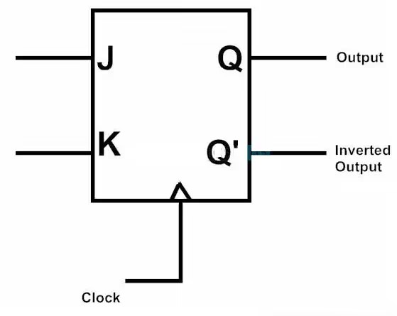
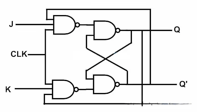
JK Flip-Flop Logic Diagram
The logic diagram of a JK flip-flop is shown below. As mentioned earlier, the JK flip-flop is an improved version of the SR flip-flop. The digital logic diagram consists of three-input NAND gates replacing the two-input NAND gates in the SR flip-flop. The inputs are changed from S and R to J and K. The digital design of the JK flip-flop store is such that one NAND gate has three inputs: J, clock signal, and feedback from Q'. Another NAND gate has three inputs: K, clock signal, and feedback from Q. This arrangement eliminates the indeterminate state present in the SR flip-flop.
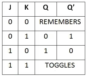
Truth Table of JK Flip-Flop
The truth table of a J-K flip flop includes the hold state, reset state, set state, and toggle state. Since it is a refinement of an SR flip flop, the truth table of the SR flip-flop is detailed into that of the J-K flip-flop.
Operating Instructions of JK Flip-Flop
Situation 1: When both inputs J and K are at a low level, Q retains its previous state, essentially maintaining the prior data.
Upon applying a digital clock pulse to the J-K flip-flop with J at a low level, regardless of other NAND gates, the output of NAND gate-1 becomes high. Similarly, if K is at a low level, the output of NAND gate-2 also remains high. Consequently, the complementary output does not change, meaning the state of the flip-flop remains unchanged.
Situation 2: When J is low and K is high, the flip-flop is in the reset state, i.e., Q=0, Q'=1.
By applying a active clock pulse to the J-K flip-flop with J input low and K input high, the output connected to the J input NAND gate turns to 1. This action resets the flip-flop to its previous state. Thus, the flip-flop enters the RESET state.
Situation 3: When J is high and K is low, the flip-flop will be in the set state, i.e., Q=1, Q'=0.
When a clock pulse is applied to the J-K flip-flop with J input high and K input low, the output connected to the K input NAND gate turns to 1. This shifts the flip-flop into a high clock input state. Hence, the flip-flop enters the SET state.
Situation 4: When both inputs J and K are high, the flip-flop is in the toggle state.
This implies that the output complements the previous state.
Clock Triggering Methods
The behavior of flip-flops is closely related to the clock signal and can be primarily classified into two common types:
1.Edge-Triggered: State updates occur only on the rising positive clock transition or negative clock transition, offering strong resistance to interference, making it suitable for high-speed circuits. Example: 74HC74 (Rising-Edge-triggered D Flip-Flop).
2.Level-Triggered: Sampling of inputs occurs continuously during either the high or low level of the clock frequency, which makes it more susceptible to interference, typically used in simple sequential circuits. Example: SR Latch.
Key Timing Parameters
Setup Time: The minimum duration for which an input signal must remain stable before the clock edge.
Hold Time: The minimum duration for which an input signal must remain stable after the clock edge.
Propagation Delay: The time taken for an active output to stabilize following a clock edge.
Application of Flip Flop
triggers find extensive utility in various domains of digital electronics. As the principal components of sequential circuits, edge-triggered flip-flops, in particular, are versatile devices employed for myriad applications such as storing binary digit, counting, and transferring binary data from one place to another.
Some of the most prevalent applications of flip-flops include counters, registers, frequency divider circuits, and data transmission. All these applications harness the clock event of flip-flops, predominantly falling within the realm of sequential circuits.
Counters
Counters are widely utilized in digital electronics and digital systems to tally the number of events occurring within a specific time frame. Often, they count the pulses entering the circuit input over a set period. In digital electronics, binary counter is a sequential circuit that generates a specific counting sequence, serving as an electronic device for counting clock signals. Counters possess memory element, essential for recalling past states of digital circuits; hence, they are constructed from flip-flops. There are two types of counters: asynchronous and synchronous. Asynchronous counters, also known as ripple counters, are formed by connecting complementary flip-flops, where the first flip-flop is linked to the clock pulse input while subsequent ones connect to the preceding flip-flop's output. In contrast, all flip-flops in synchronous counters are connected to the same clock signal, triggering simultaneously, thereby earning the moniker "synchronous counters."
Registers
A flip-flop can store a single bit of data, either a 1 or 0. Registers, however, are used to store multiple bits of data, hence the need for flip-flops in their circuit design. In digital electronics, a register serves as a device for storing information. Given that a solitary flip-flop permits 1-bit storage, n flip-flops are connected in sequence to store n bits of data. For instance, if a computer needs to store 16 bits of data, it requires a set of 16 flip-flops. The inputs and outputs of a register can be either serial or parallel, based on requirements. The series of data bits stored in a register is termed a “byte” or “word.” When multiple flip-flops are linked together, this structure is called a register. Information stored can be transferred within the register, with such registers being referred to as “shift registers.” Asynchronous and synchronous registers: Shift registers, composed of flip-flops, operate based on the state of the flip-flops. Registers functioning asynchronously are called “asynchronous shift registers.” Similarly, shift registers that change state only when triggered by a clock pulse are dubbed “synchronous shift registers.”
Frequency Divider Circuit
As the name suggests, a frequency divider circuit is used to produce a digital output signal output exactly half the input frequency. Frequency divider circuits are typically used in designing asynchronous counters. The process of dividing or reducing the output frequency to half of the variably-timed input signal frequency is known as “frequency division.” This means that if we handle an input signal with a frequency of 160k Hz, the frequency divider circuit will provide an output stage of 80k Hz.
Data Transmission
“Data transmission” is the process of transferring data from one register to another. Generally, shift registers perform this type of operation. Data can be transferred via flip-flops in two ways: serial data transfer and parallel data transfer.
The essence of a flip-flop lies in its ability to update states through active clock signals, converting input signals into stable outputs at specific moments. Its design requires balancing speed, power consumption, and interference resistance, making it a fundamental component in digital systems for achieving synchronous control logic, state storage registers, and reference timing signal. Understanding the timing parameters of flip-flops, such as setup and hold times, is crucial to preventing control circuit metastability and errors.