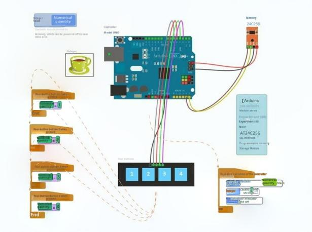
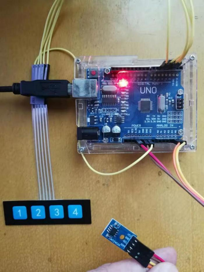
Arduino Hands-On - AT24C256 Storage Module
Experiment: AT24C256 I2C Interface EEPROM Storage Module
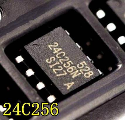
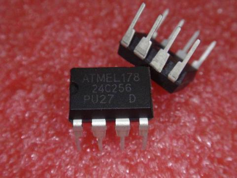
AT24C256is a 256Kbit serial electrically erasable programmable read-only memory (EEPROM) from ATMEL. It comes in an 8-pin dual in-line package with features such as compact structure and large storage capacity. Multiple ICs can be connected in parallel on a 2-wire bus, making it especially suitable for data acquisition systems with high-capacity storage requirements. AT24C256 is packaged in SOP-8 format.
Chip Specifications
The chip operates at three different voltages:
• 5.0V (VCC=4.5V~5.5V)
• 2.7V (VCC=2.7V~5.5V)
• 1.8V (VCC=1.8V~3.6V)
Features:
• Internally organized as 32k×8 memory units
• 2-wire serial interface
• Schmitt trigger with filtered input to suppress noise
• Bidirectional data transfer protocol
• Hardware write protection pin and software data protection function
• Supports 64-byte page write mode
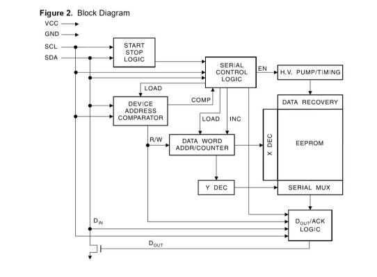
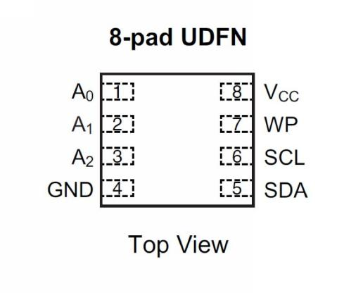
• A0, A1: Address selection input pins. In a serial bus structure, up to 4 AT24C256 ICs can be connected. A0 and A1 are used to differentiate between each IC. A0 and A1 are grounded when not in use.
• SCL: Serial clock input. Data on SDA is written into the memory on the rising edge, and data is read from the memory to SDA on the falling edge.
• SDA: Bidirectional serial data input/output port. Used for data exchange between the memory and microcontroller.
• WP: Write protection input. When this pin is connected to ground, write operations are allowed; when connected to VCC, all write memory operations are disabled. If left unconnected, the pin is internally pulled down to ground.
• VCC: Power supply.
• GND: Ground.
• NC: Not connected.
Operating Principle of AT24C256
The AT24C256 has 512 pages, with each page containing 64 bytes. The address for any unit is 15 bits long, ranging from 0000H to 7FFFH.
Chip Operating States:
Clock and Data Transfer
In general, SDA is pulled high by external devices. Data transmission occurs when SDA changes while SCL is low, indicating the intention to transfer data. When SCL is high and SDA changes, it indicates a change in status.
Start State (START)
When SCL is high and SDA transitions from high to low, it signifies the start of data transmission. This state must occur before all commands.
Stop State (STOP)
When SCL is high and SDA transitions from low to high, it indicates the end of data transmission.
Acknowledge State (ACK)
All addresses and data are serially transmitted to or read from the memory in 8-bit form. The memory responds with a zero on SDA during the 9th clock cycle to indicate that it has received the 8 bits of data. See the bus protocol diagram for reference.

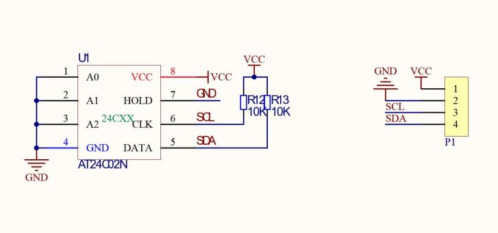
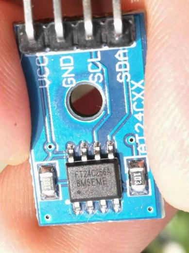
AT24C256 I2C Interface EEPROM Storage Module
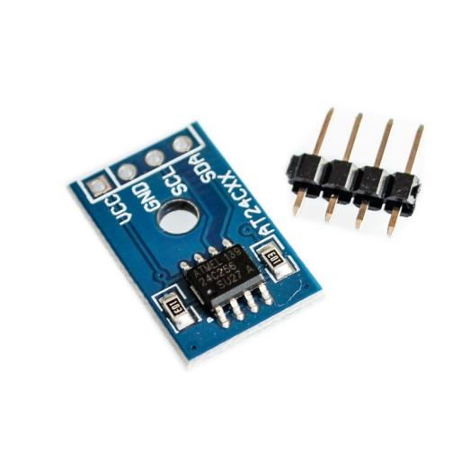
1. On-board imported AT24C256 chip;
2. On-board pull-up resistors required for I2C communication;
3. All pins are led out and labeled;
4. PCB board size: 1.9(CM) x 1.1(CM)

Module Electrical Schematic