What is Phototransistor?
What is Phototransistor?In the vast landscape of electronics, components that bridge the physical and digital worlds are fundamental. Among these, the phototransistor stands out as a remarkably simple yet powerful electronic device for detecting and converting light into an electrical signal. It's a cornerstone of optoelectronics, finding its way into countless applications from industrial automation and consumer electronics to semiconductor devices and security systems. But what exactly is a phototransistor, and how does it fulfill this critical sensing role?
Core Concept: A Transistor Awakened by Light
At its heart, a bipolar phototransistor is fundamentally a bipolar junction transistor (BJT) – specifically, usually an NPN type – with one crucial modification: its base-collector junction is physically exposed to incident light. Instead of relying solely on an electric current injected into the base terminal to control the much larger current flowing between collector and emitter, a modern phototransistor harnesses the light energy of photons.
The Inner Workings: From Photons to Current
The magic happens through the photoelectric effect applied to semiconductor materials:
1.The Sensitive Junction: The base-collector junction is reverse-biased in normal modern of operation (positive voltage on the collector relative to the emitter terminal, common base often left floating or connected via a dependent resistor).
2.Photon Absorption: When incident light (photons) with electromagnetic energy strikes the exposed base-collector junction (the depletion region), it transfers electrical energy to electrons within the semiconductor crystal lattice.
3.Electron-Hole Pair Generation: This electric energy excites electrons, causing them to break free from their atomic bonds, creating mobile negative charge carriers (electrons) and leaving behind positive charge carriers (holes).
4.Base Current Generation: These photogenerated electron-hole pairs are swept apart by the electric field present in the reverse-biased depletion region. Electrons are pulled towards the collector (positive), while holes move towards the base region.
5.Amplification: This movement of holes into the base region effectively acts like a positive base current (I_B). Crucially, the ordinary transistor structure provides amplification. A small photogenerated base current controls a much larger collector current (I_C). The relationship is I_C = β * I_B, where β (beta) is the normal transistor's current gain, typically ranging from 100 to over 1000 for range of phototransistors. This internal amplification is the key advantage over a simple photodiode.
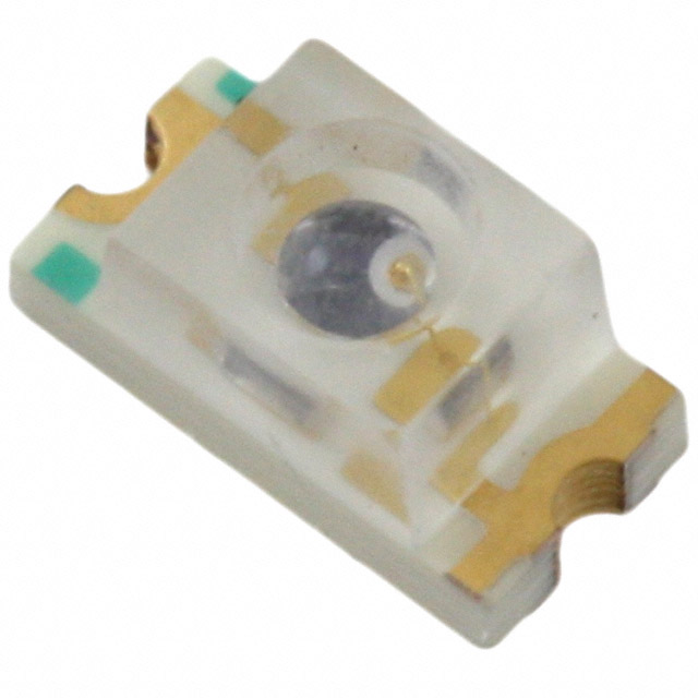
Visualizing the Structure:
● Case: Often transparent (clear epoxy) or has a lens to focus light pulses onto the chip.
● Chip: The semiconductor die where the NPN layers are fabricated.
● Exposed Junction: The sensitive collector-base junction is positioned under the light entry point.
● Terminals: Collector (C) and Emitter (E) are the base connection points. The Base terminal may be absent or available for biasing adjustments but is often left unconnected.
Key Characteristics and Advantages:
1.High Sensitivity: Due to the internal current gain (β), types of phototransistors produce significantly larger output current for a given light intensity compared to photodiodes. This makes them excellent for detecting low light levels.
2.Simplified Circuitry: The built-in amplification often eliminates the need for an external amplifier circuit diagram required by photodiodes, simplifying design and reducing electronic component count and cost.
3.Cost-Effectiveness: They are relatively inexpensive and readily available modern components.
4.Ruggedness: Simple structure lends itself well to robust packaging.
5.Fast Response (for many applications): While generally slower than PIN photodiodes (response times in microseconds vs. nanoseconds), photodarlington-type transistor are fast enough for a vast array of applications like light detection, speed sensing, and basic communication.
Limitations and Trade-offs:
1.Slower Speed: The gain mechanism inherently involves charge storage in the base region, limiting switching time compared to photodiodes. Not ideal for very high-frequency light modulation (e.g., high-speed fiber optics).
2.Temperature Sensitivity: Like all BJTs, gain (β) and dark current are temperature-dependent, which can affect performance stability in extreme environments.
3.Saturation: At high light intensities, the output current saturates and becomes non-linear with increasing light.
4.Limited Spectral Range: Responsivity is typically optimized for visible light (especially near-infrared, around 850-950 nm, common with IR LEDs) but falls off sharply outside this range compared to specialized photodiodes. Filtering is often used.
5.Dark Current: A small leakage current flows even in complete darkness, which can introduce noise.
Phototransistor vs. Photodiode: Choosing the Right Tool
● Use a Phototransistor when: High sensitivity is paramount, phototransistor circuit simplicity is desired, cost is a factor, and speed requirements are moderate (kHz to low MHz range). Examples: Object presence detection (slots, conveyors), opto-isolators, simple remote controls, light barriers, twilight sensors, basic pulse counting.
● Use a Photodiode (often with an amplifier) when: Very high speed (MHz to GHz) is needed, linear response over a wide range is critical, precise low-light measurement is required, or operation outside the visible/near-IR spectrum is necessary. Examples: High-speed data communication (fiber optics), precision light meters, spectroscopy, laser rangefinding.
Common Applications: Where You Find Them
Phototransistors are ubiquitous:
● Industrial Automation: Object counting, position sensing, limit optical switches, paper detection in printers/copiers, rotary encoder disks.
● Opto-Isolators (Optocouplers): Providing electrical isolation between electronic circuits while allowing signal transfer via light (an LED shines on the phototransistor).
● Consumer Electronics: Remote control receivers (detecting IR pulses from the remote), CD/DVD player lens position detection, automatic brightness control in displays, smoke detectors (interrupted light beam).
● Security Systems: Intrusion detection beams, card readers.
● Medical Devices: Pulse oximetry (indirectly, though often photodiodes are used now), fluid level detection.
● Automotive: Rain sensors (light scatter detection), twilight sensors for automatic headlights.
Variations and Enhancements:
● Darlington Phototransistor: Two regular transistors cascaded internally for even higher gain (β²), providing extreme sensitivity but slower speed.
● Photodarlington: Similar concept, often a single package integrating a photodiode driving a discrete transistor action.
● IR Phototransistors: Specifically optimized for high sensitivity in the near-infrared range.
● Lensed Types: Focus light onto the sensitive area for longer range or directionality.
Conclusion: A Pillar of Optosensing
The phototransistor remains an indispensable component in the engineer's toolkit. Its elegant fusion of the photoelectric effect with the amplifying power of the type of transistor creates a optical sensor that is sensitive, relatively simple to use, and cost-effective. While it may cede ground to photodiodes in ultra-high-speed or ultra-precise applications, its inherent amplification and robustness ensure its continued dominance in countless everyday sensing tasks where detecting the presence, absence, or intensity of light reliably and economically is the primary goal. From the humble garage door opener to complex factory robots, the phototransistor silently and efficiently translates the world of light into the language of electricity.