In-Depth Analysis of Monostable Multivibrators
Fundamental Concepts of Monostable Multivibrators
-
What is a monostable multivibrator?
A monostable multivibrator is an electronic circuit characterized by monostable behavior, primarily used to generate timing pulses or implement signal delay functions.
A monostable multivibrator maintains only one stable state. When triggered by an external signal, it briefly enters an unstable state (quasi-stable state) before automatically returning to its stable state after a preset duration. For example, supermarket automatic doors closing after being opened exemplify this typical monostable application.
-
What are the main characteristics of a monostable multivibrator?
(1) Single stable state
This is the most fundamental characteristic of a monostable multivibrator, and the origin of its name, "monostable." Without any external trigger signal, the circuit remains stably predefined, typically outputting a low level (i.e., 0). This stable state is its eternal "home", to which it always returns.
(2) Requires an external trigger signal
The circuit will not change state automatically; it must be initiated by an external pulse (trigger signal). This trigger signal is typically a pulse with a very steep edge, such as the instant a button is pressed or the rising/falling edge of a digital signal.
(3) A quasi-steady state
When triggered, the circuit transitions from its stable state to another state (typically switching the output to a high level, i.e., 1). However, this state is temporary and unstable, referred to as a "quasi-steady state" or "transient state." The circuit cannot remain in this state for an extended period of time.
(4) Automatic return to steady state
After maintaining a steady state for a fixed period, the circuit will automatically return to its unique stable state without any external intervention. This return process is determined by the internal timing elements within the circuit (typically an RC circuit).
(5) Generate output pulses of fixed width
From the moment it is triggered into quasi-steady state until it automatically returns to steady state, the circuit outputs a rectangular pulse with a fixed width (duration). This pulse exhibits a regular waveform with steep edges.
-
What is the difference between a monostable multivibrator and a bistable multivibrator?
Monostable and multistable multivibrators are two circuits with fundamentally different functions. Simply put, the core distinction lies in the number of stable states they possess:
(1) Monostable
There is only one stable state. The output typically remains stable in one state (such as a low level). When triggered externally, it temporarily transitions to another state (high level) but automatically reverts to its original stable state. It generates pulses of fixed width.
(2) Bistable
There are two stable states. The output can remain stably at either a high or low level for extended periods. An external trigger signal is required to switch it between the two states. It is a memory unit (1-bit memory), such as an SR latch.
Gain a deeper understanding of their differences through a detailed comparison chart:
|
Characteristics |
Monostable Multivibrator |
Bistable Multivibrator |
|
Aliases |
Single-shot, Delay element |
Latch, Flip-flop (e.g., SR latch) |
|
Number of Steady States |
One |
Two |
|
Output Behavior |
Normally stable in one state (e.g., low level). Upon triggering, the output transitions to a transient state (high level) and automatically returns to the stable state after a fixed duration. |
The output can remain indefinitely in either the high or low state until a trigger signal commands a change. |
|
Triggering Method |
Requires an external trigger pulse to initiate a cycle. |
Requires an external trigger pulse to switch states. |
|
Output Waveform |
Generates rectangular pulses with fixed width and amplitude. The output pulse width is determined by the circuit's inherent RC time constant and is independent of the trigger pulse width. |
The output exhibits a step-change voltage level. The output state is determined by the input signal. |
|
Core Functions |
Timing, delay, pulse shaping (converting irregular input pulses into regular square waves). |
Stores 1-bit binary data (0 or 1), counting, switch debouncing. |
|
Circuit Core |
Typically, an RC timing circuit determines the transient time. |
Positive feedback is usually formed by two cross-coupled inverters (or transistors), creating two stable points. |
|
Analogy |
A self-closing door: Push it (trigger), and it opens for a while before closing on its own. |
A light switch: Press it (trigger) to turn on, press it again (trigger) to turn off. It can “remember” its current state. |
|
Application Examples |
1. Generate fixed-width pulse signals. 2. Serve as delay circuits (triggering other circuits using the edges of output pulses). 3. Shape irregular pulses from sensors (e.g., button presses) into regular pulses recognizable by MCUs. |
1. SR latches eliminate mechanical switch bounce. 2. Form the basic building blocks of digital circuits like registers and memory. 3. Function as binary dividers and counters |
-
Common Circuit Diagrams for Monostable Multivibrators
The operating principle of a monostable multivibrator involves a flip-flop, a capacitor, and two Zener DIODES. When a trigger signal is input, it causes the flip-flop to toggle, charging and discharging the capacitor through the Zener diodes with different time constants. This generates a steady-state pulse signal at the output with a fixed width and duration.
The purpose of a monostable multivibrator is to simulate complex oscillation systems. It can be used to study the characteristics of complex oscillation systems, as well as the stability of these systems and the factors that affect their stability. It can also simulate the response of complex oscillation systems and the control strategies for oscillation systems. Furthermore, monostable multivibrators have extensive applications in digital circuits, where they can generate the trigger signals and clock signals required for sequential logic circuits.
The circuit below represents a monostable multivibrator. Also known as a monostable multivibrator or timer, its primary function is to generate pulses of fixed width. The pulse width is determined by the component values selected during circuit design.
The primary component of this circuit is the LM139, and only one section of four LM139s is utilized. The values of C2 and R1 determine the pulse width of this circuit. When selecting the value of R1, it should be at least 10 times that of R4 to avoid load effects.
The monostable multivibrator circuit is also known as a monostable multivibrator or timer. Its function is solely to generate a fixed-width pulse, independent of the width of the trigger input pulse.
When triggered, the monostable multivibrator generates a fixed-width pulse at its output. This fixed-width output remains consistent regardless of the width of the input trigger pulse.
The schematic diagram below illustrates an example of a monostable multivibrator circuit utilizing the LM139 as the primary active component.
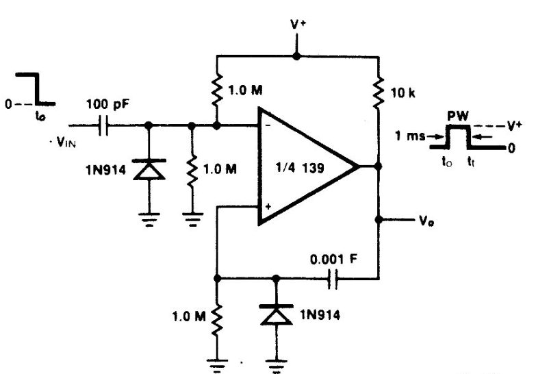
The output pulse width is determined by the 0.001μF capacitor and the 1 MΩresistor (Rp) connected to the non-inverting input. The 10k resistor connected to the op-amp output serves as a pull-up resistor. The cycle-determining resistor (Rp) should be selected to be at least 10 times larger than the pull-up resistor to avoid loading the output. The voltage divider resistors at the inverting input determine the minimum trigger amplitude level.
By selecting the period to balance the thermal coefficients of the resistor and capacitor, or by using components with very low temperature coefficients if an imbalance exists, the thermal stability of the output pulse width can be maintained at a low level. The width of the output pulse from this monostable multivibrator will be independent of the voltage source. We anticipate that changes in pulse width caused by variations in the 5V power supply voltage will be less than 2%.
A monostable multivibrator is an electronic circuit that generates a single pulse each time it is triggered. This circuit is sometimes referred to as a "monostable multivibrator." It is beneficial, for example, in generating delays for timing applications or debouncing mechanical switches to ensure only one rising edge and one falling edge occur each time the switch closes.
In a discrete circuit, the left transistor is typically on, while the right transistor is off. When the base of the switch transistor is pressed, the on transistor turns off, and the collector voltage rises. As the collector voltage increases, the capacitor begins charging through the base of the opposite transistor. Consequently, it turns on and produces a low-level state at the output. To maintain output saturation, the low output state keeps the left transistor off until the capacitor current drops below a threshold. As the output side begins to turn off, the left transistor returns to the on state due to the rising voltage. Its collector voltage is low. Thus, the capacitor discharges through the 10K resistor (emitter to base). The circuit then remains stable until the following input.
Note: These circuits are not retriggerable. If triggered before the timing capacitor discharges, the output duration will be shorter than usual, requiring approximately the same time as the output.
When triggered, the monostable multivibrator circuit produces a fixed pulse width. The input is fed to an open-collector source because TR1 shorts the input to ground during the active state on the circuit's output.
The circuit's output is derived from the collector of TR2. The pulse width of this monostable multivibrator output can vary between 0.5 and 300 milliseconds, adjustable via the 1M trimmer potentiometer R5.
Operating Principle of a Monostable Multivibrator
-
What is the triggering mechanism of a monostable multivibrator?
The vast majority of monostable circuits employ edge triggering rather than level triggering. This means the circuit is sensitive to the transition of the input signal (from high to low or from low to high), not to the signal's level. Using edge triggering ensures the output pulse width is entirely determined by the circuit's own RC timing elements, independent of the triggering pulse's width. Even if the trigger signal is a long, low-level signal, the circuit triggers only once at the instant of its falling edge, outputs a pulse of fixed width, and then returns to steady state, preventing the possibility of multiple triggers.
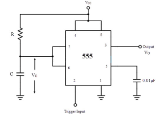
The most common monostable circuit is built using a 555 timer. We use its falling-edge trigger mechanism as an example to illustrate:
Structure: The TRIG pin (Pin 2) of the 555 timer is the trigger input. An external RC network connects between DISCH (pin 7) and THRES (pin 6), and is connected to Vcc. The output (pin 3) generates pulses.
Triggering Process: Without triggering, the TRIG pin remains high (> 1/3 Vcc). At this time, the output is low, the internal discharge transistor conducts, and the voltage across capacitor C is clamped to 0V. This is the circuit's only stable state. When an external pulse is applied to the TRIG pin, the trigger comparator flips upon its falling edge, dropping below 1/3 Vcc. This falling edge below 1/3 Vcc constitutes the valid trigger signal. The trigger signal causes the output to immediately transition to a high level, simultaneously turning off the internal discharge transistor. Capacitor C begins charging toward Vcc through resistor R. From the moment of triggering, a fixed timing cycle commences. The output remains high. When the capacitor voltage charges to more than 2/3 Vcc, the threshold comparator toggles, forcing the output back to low. Simultaneously, the discharge transistor turns on again, rapidly discharging capacitor C to 0V. The circuit automatically returns to its stable state and awaits the next trigger pulse.
The triggering mechanism of a monostable multivibrator essentially works as follows: a qualifying edge signal (typically a falling edge) disrupts the circuit's equilibrium, initiating its inherent RC timing process. This generates an output pulse with a fixed width that is independent of the triggering signal. This mechanism makes monostable circuits highly suitable for converting irregular input events into regular, predictable output pulses, finding extensive applications in timing, delay, and pulse shaping.
-
Steady-State and Transient Analysis of Monostable Multivibrators
Let's continue analyzing the example of a monostable circuit built with a 555 timer:
(1) Steady-state analysis
- Steady state is the long-term condition maintained by a circuit without external triggering.
- Output state: The output (Vout) is at a low level (0V).
- Internal state: Since the trigger pin (TRIG) has no valid input, it is typically held at a high level (> 1/3 Vcc) by a pull-down resistor, and the internal trigger comparator outputs "0".At this point, the discharge transistor (DISCH) saturates, effectively shorting pin 7 to ground.
- Capacitor state: One terminal of capacitor C is connected to ground via pin 7, so the voltage across the capacitor, Vc, is approximately 0V. Since Vc (connected to the THRES pin) is less than 2/3 Vcc, the internal threshold comparator output is also "0".
- Summary: This is a stable, self-sustaining state. All forces are in equilibrium: the circuit will indefinitely maintain this state until a valid trigger signal arrives.
(2) Transient Analysis
A transient state refers to the temporary state a circuit enters upon triggering, which cannot be sustained in the long term and automatically reverts to a steady state upon completion.
Phase 1: Trigger Initiation (at time t₀)
Trigger Event: A negative pulse (falling edge) arrives at the TRIG pin, and the voltage drops below 1/3 Vcc.
State Inversion: The trigger comparator inverts, outputting "1" to set the internal RS flip-flop. The output (Vout) immediately transitions to a high level. The Q-NAND output of the RS flip-flop goes low, forcing the discharge transistor to turn off (cut off).
Timing Start: After the discharge transistor turns off, pin seven is disconnected from ground, and capacitor C begins charging from Vcc through resistor R. From this moment, the timing cycle begins.
Phase 2: Timing Process (t₀ → t₁ period)
Capacitor Charging: The capacitor voltage, Vc, rises exponentially from 0V toward Vcc. Its value is Vc = Vcc * (1 - e^(-t/RC)).
Output Hold: During this phase, as long as Vc < 2/3 Vcc, the threshold comparator outputs "0" and does not alter the RS flip-flop state. Thus, the output remains high.
Core characteristic: The width of the output pulse depends on the time required for the capacitor voltage to charge from 0V to 2/3 Vcc.
Phase Three: Auto-Reset (at time t₁)
Threshold Comparison: When the capacitor voltage Vc rises to at least 2/3 Vcc, the threshold comparator (THRES) toggles and outputs a "1".
State Flip: This resets the RS flip-flop. The output (Vout) immediately transitions back to its low state. The Q non-gate goes high, causing the discharge transistor to re-saturate and turn on.
Transient End: The output transitions to a low level, marking the end of the transient.
-
Timing and Waveform Output of Monostable Multivibrator
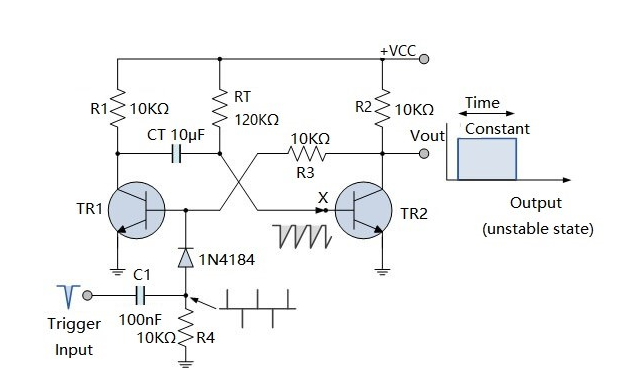
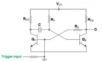
The basic collector-coupled transistor monostable multivibrator circuit, along with its associated waveforms, is shown above. When the power supply is turned on, the base of transistor TR2 is connected to Vcc via the bias resistor RT, causing the transistor to conduct thoroughly and enter saturation. Simultaneously, TR1 turns off during this process, representing the steady state of the zero-output circuit. Therefore, the current flowing into the saturated base of TR2 will be: Ib = (Vcc - 0.7) / RT.
Suppose a negative trigger pulse is now applied to the input. In that case, the pulse's fast-falling edge will directly charge capacitor C1, causing it to reach the transistor base and turn on TR1 via the blocking diode. The voltage at the collector of TR1 rapidly drops below zero volts, effectively causing capacitor CT to reverse charge to -0.7V. This operation results in a negative base voltage at point X for transistor TR2, effectively turning the transistor off. This represents the circuit's second state, the unstable state, where the output voltage equals Vcc.
The timing capacitor CT begins discharging this -0.7V current through the timing resistor RT, attempting to charge back to the supply voltage Vcc. The negative voltage at the base of transistor TR2 starts to combine with RT and CT. As the base voltage of TR2 rises back to Vcc, the transistor conducts, thereby turning off transistor TR1 once more. Consequently, it automatically returns to its original stable state within the monostable multivibrator, awaiting a second negative trigger pulse to restart the process.
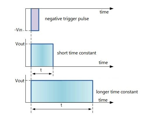
A monostable multivibrator can generate short pulses or long rectangular waveforms. The rising edge of the wave rises with time and the externally applied trigger pulse, while its falling edge depends on the RC time constant of the feedback element. This RC time constant can vary over time, producing a series of pulses. Compared to the original trigger pulse, these pulses exhibit a controlled, fixed time delay, as shown below.
The time constant of a monostable multivibrator can be altered by changing the values of capacitor CT and/or resistor RT. Monostable multivibrators are commonly used to increase pulse width or introduce delays in circuits. The output signal's frequency always matches that of the trigger pulse input, differing only in pulse width.
Circuit Implementation of a Monostable Multivibrator
-
Transistor Monostable Circuit
A transistor monostable circuit is a pulse-generating circuit featuring both steady-state and transient-state characteristics. Its core component is a transistor, and it is commonly used in applications such as pulse shaping and timing.
(1) RC Time Constant Calculation
A monostable multivibrator has one stable state and one transient state. When triggered by an external pulse, it flips from the stable state to the transient state. After maintaining the transient state for a period of time (Tw), it automatically returns to the stable state. The duration of this transient state—that is, the width of the output pulse—is entirely determined by the externally connected resistor (R) and capacitor (C).
- Core Calculation Formula
The formula for calculating the output pulse width (also known as the delay time) is:
T≈0.693×R×C
Or more generally expressed as: T = ln(2)×R×C
Where:
T is the output pulse width or delay time, measured in seconds (s).
R is the timing resistor, measured in ohms (Ω).
C is the timing capacitance, measured in farads (F).
ln(2) is the natural logarithm, approximately equal to 0.693.
This formula derives from the voltage curve of a capacitor charging through a resistor and the circuit's threshold voltage for switching (typically 2/3 of the supply voltage).
- Calculation Steps and Example
Suppose you need to design a monostable circuit with a pulse width of 10 milliseconds (i.e., 0.01 seconds).
First, select the capacitance value (C): Typically, start by choosing a capacitance value within a reasonable range. The capacitance should not be too small (prone to parasitic capacitance effects) or too large (causing significant leakage current). We select a common value of 10μF.
C = 10μF = 0.00001 F
Next, calculate the resistance value (R):
Using the formula T = 0.693×R×C
Rewrite as: R = T / (0.693×C)
Substitute values: R = 0.01 / (0.693×0.00001)
Calculation: R = 0.01 / 0.00000693≈1443Ω
Then select a standard resistor: The calculated 1443Ωis not a standard value. We can choose the closest standard resistor value, such as 1.5 kΩ.
Finally, verify the actual pulse width:
Calculate the actual pulse width using the standard resistor value: T = 0.693×1500×0.00001
T≈0.010395 s≈10.4 ms
This result is very close to our design target of 10 ms, meeting the requirements for most applications.
(2) Waveform Simulation Example
The pulse generator shown below is an example of a monostable multivibrator circuit.
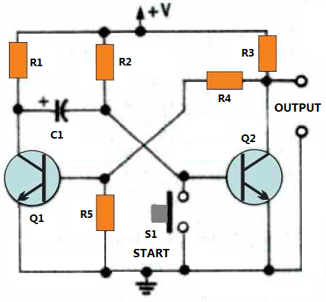
Under normal conditions, R2 drives transistor Q2 into saturation, producing a low output (from the collector of transistor Q2). In this state, transistor Q1 (whose base is biased via the collector of transistor Q2 and resistor R4) turns off, with its collector now at 100% supply voltage.
When switch S1 is briefly closed, the START signal is applied to Q2. Q2 turns off, forcing the output to a high level and turning on Q1 via R4. The opening of S1 triggers the regenerative switching action.
During the regenerative reaction, the charge on C1 drives the base of transistor Q2 to a negative potential.
C1 begins discharging through R2. Its charge eventually drops to the point where Q2 turns on again, triggering another regeneration reaction.
Subsequently, the output pulse ceases, both transistors return to their original states, and the circuit's activity comes to a close.
Thus, when an input trigger signal is applied by momentarily closing switch S1, the output of the monostable multivibrator circuit generates a positive pulse. The values of R2 and C1 determine the pulse period.
The following equation expresses this relationship: Pulse Period = -0.7 × R2 × C1.
Pulse duration is measured in microseconds, C in microfarads, and R in kiloohms. Activating the momentary switch or supplying an input command signal triggers the circuit shown in Figure 2.
A negative pulse applied to the base of Q2 or a positive pulse applied to the base of Q1 can serve as the trigger signal. The figure below shows an actual design of a mechanically triggered monostable multivibrator. This multivibrator can be initiated by sending a positive pulse to the base of Q1 through R2 via the momentary switch S1.
The circuit waveforms are shown in the figure below. During operation, the base-emitter junction of Q2 is reverse-biased with a peak voltage equal to the supply voltage, as illustrated.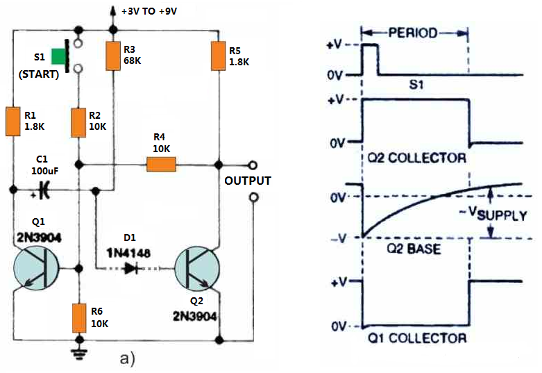
This means that to prevent damage to the transistor, the maximum supply voltage must be limited to approximately 9 volts.
By connecting silicon diode D1 in series with the base of Q2, a supply voltage exceeding the reverse base-emitter breakdown voltage of Q2 can be reliably provided, as shown in the diagram.
In the circuit, the resistance value of timing resistor R3 must be significantly greater than R1, yet lower than the product of R5 and Q1's hFE. The pulse duration in the above diagram is 50 milliseconds divided by the capacitance value of C1 (in microfarads). With C1 set as shown, the pulse timing output is 5 seconds.
-
Operational Amplifier Monostable Circuit
The operational amplifier monostable multivibrator (MMT) circuit is a positive feedback (or regenerative) switching circuit with only one stable state, generating an output pulse of specified duration T.
An external trigger signal is applied to change the state. After a set duration (measured in microseconds, milliseconds, or seconds), determined by the RC components, the monostable circuit returns to its original stable state. This state persists until the next trigger input signal arrives.
The basic monostable multivibrator block diagram is as follows: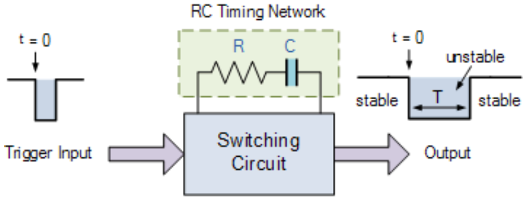
The block diagram above shows that a monostable multivibrator can be constructed by adding an external resistor (R) and capacitor (C) across the terminals of a switching circuit. The switching circuit can be implemented using transistors, digital logic gates, or general-purpose operational amplifiers. The time constant τ of the resistor-capacitor combination determines the pulse width T.
In this tutorial, we will build a monostable multivibrator circuit using an operational amplifier comparator circuit with a positive feedback path. Because the feedback is positive, the circuit is regenerative, meaning it amplifies the differential input signal.
Operational Amplifier Monostable Circuit
First, let's consider the inverting amplifier circuit shown in the figure.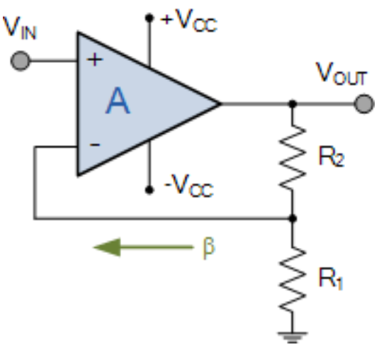
In this inverting operational amplifier configuration, a portion of the output signal (referred to as the feedback fraction) is fed back to the amplifier's inverting input through a resistor network.
Consequently, in this fundamental inverting configuration, the feedback fraction is negative when fed back to the inverting input. This negative feedback arrangement between the output and inverting input terminals forces the differential input voltage to tend toward zero.
The result of this negative feedback is that the operational amplifier produces an amplified output signal that is 180 degrees out of phase with the input signal. Therefore, an increase in the voltage -V at the non-inverting terminal, which is fed back from the output, causes a decrease in the output voltage V_O, resulting in a balanced and stable amplifier operating within its linear region.
Now consider the same operational amplifier circuit where the non-inverting and inverting inputs are swapped. That is, the feedback signal is fed back to the non-inverting input, making the feedback process positive. This creates a basic operational amplifier comparator circuit with built-in hysteresis.
The operational amplifier monostable multivibrator circuit is built around an operational amplifier configured as a closed-loop Schmitt trigger circuit. This circuit utilizes positive feedback provided by resistors R1 and R2 to generate the desired hysteresis. The use of positive feedback means the feedback is regenerative and provides the required state dependency, effectively transforming the operational amplifier into a bistable storage device.
Consider the basic operational amplifier voltage comparator circuit below.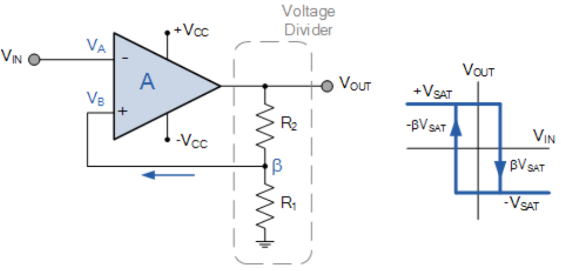
A resistor network is connected between the operational amplifier's output and its non-inverting (+) input. When Vout saturates toward the positive supply rail (+Vcc), a positive voltage relative to ground is applied to the operational amplifier's non-inverting input. Similarly, when Vout saturates toward the negative supply rail (-Vcc), a negative voltage relative to ground is applied to the operational amplifier's non-inverting input.
Because the two resistors are connected across the output as a voltage divider network, the voltage V_B appearing at the non-inverting input depends on the ratio of the two resistors relative to the output voltage being fed back. This feedback fraction β is expressed as: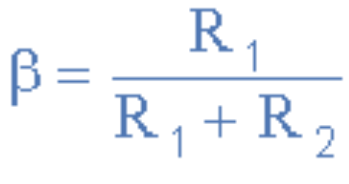
Note that we can make the value of β variable by replacing resistors R₁ and R₂ with a potentiometer. In this potentiometer, the tap is directly connected to the non-inverting input of the operational amplifier, allowing us to alter the feedback fraction.
Since the hysteresis amount is directly proportional to the feedback fraction, it is best to avoid constructing Schmitt trigger operational amplifiers (regenerative comparators) with very small hysteresis (small β), as this may cause the operational amplifier to oscillate between the upper and lower setpoints during switching.
By placing a feedback network between the output and the inverting (-) input of the Schmitt trigger, we can control the time it takes for the Schmitt trigger operational amplifier to change states. In this manner, the op-amp itself generates a signal at its inverting input through an external RC feedback network, as illustrated in the figure.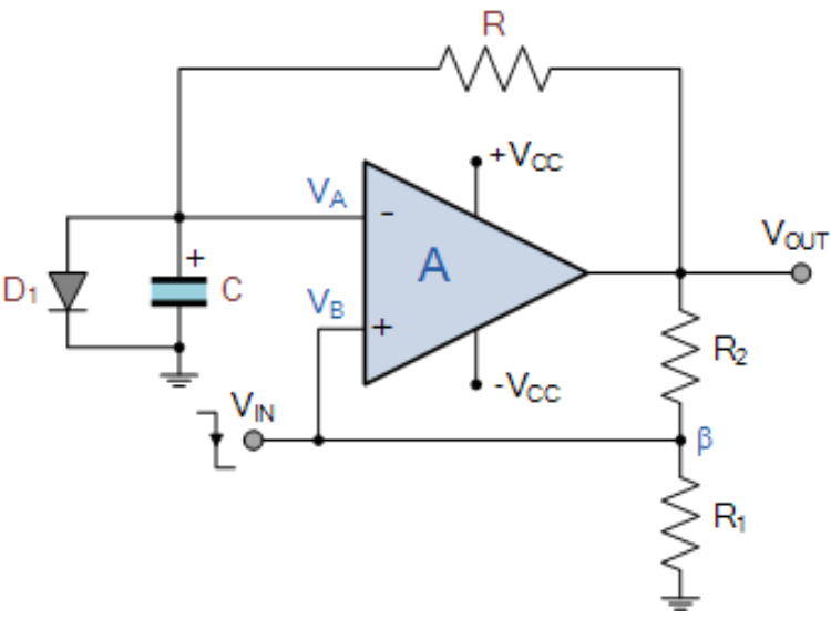
At initial power-up (i.e., t = 0), the output (V OUT) will saturate toward either the positive supply rail (+Vcc) or the negative supply rail (-Vcc), as these are the only two stable states permitted for the operational amplifier. Now, let us assume the output has swung toward the positive supply rail +Vcc. Then, the voltage V_B at the non-inverting input will equal +V_cc * β, where β is the feedback fraction.
The non-inverting input remains at 0.7 volts—the forward voltage drop across diode D₁—and is clamped to 0V (ground) by diode D₂ to prevent it from becoming positive.Thus, the potential at VA is significantly less than that at VB, stabilizing the output at +Vcc. Simultaneously, capacitor (C) charges to the same 0.7V potential and is held there by the forward voltage drop across the diode.
If we apply a negative pulse to the non-inverting input, the 0.7V voltage at VA now becomes greater than the voltage at VB because VB is now negative.Consequently, the output of the Schmitt trigger configuration operational amplifier switches state and saturates toward the negative supply rail -Vcc. The result is that the potential at V_B now equals -Vcc * β.
This transient metastable state causes the capacitor to charge exponentially in the opposite direction, from +0.7 volts down to the newly saturated output, -Vcc, through the feedback resistor R. Diode D₁ becomes reverse-biased and thus inactive. Capacitor C discharges with a time constant τ = R * C.
Once the capacitor voltage at V_A reaches the same potential as V_B, namely -V_cc * β, the operational amplifier returns to its original, permanent stable state, and the output again saturates at +V_cc.
Note that once the timing cycle completes and the op-amp output reverts to its steady state, saturating toward the positive rail, the capacitor attempts to reverse-charge toward +Vcc but can only charge up to a maximum of 0.7V—the forward voltage drop imposed by the diode. This effect can be graphically illustrated: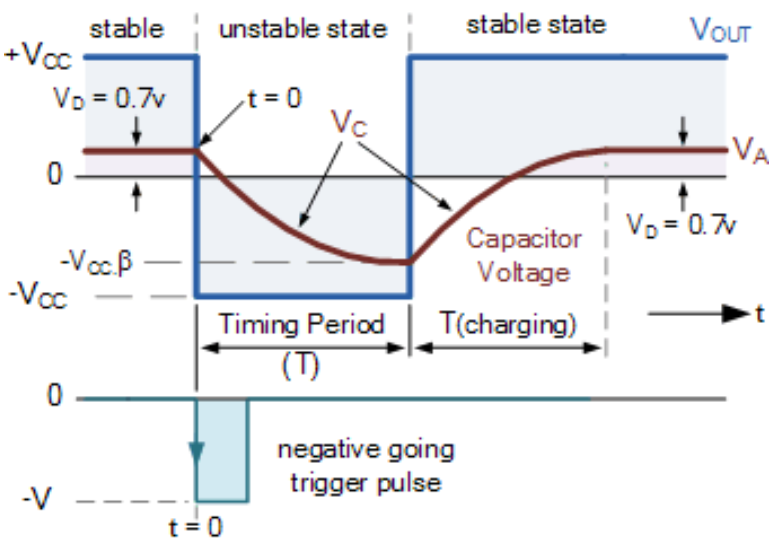
Then we can see that the negative trigger input will switch the operational amplifier monostable circuit to its temporary unstable state. After a delay period T, capacitor C charges through the feedback resistor R. Once the capacitor voltage reaches the required potential, the circuit returns to its normal stable state.
This delay time (T) of the output square wave, i.e., the unstable state duration, is:
If the feedback resistors of two operational amplifiers have identical values, i.e., R₁ = R₂, then the above equation can also be simplified to:
Clearly, the capacitor requires time to recharge from -Vcc * β back to V_D (0.7V); therefore, during this interval, a second negative pulse may fail to initiate a new timing cycle.
To ensure the operational amplifier monostable circuit functions correctly when the next trigger pulse is applied, the time interval (T_(total)) between trigger pulses must exceed the timing duration T plus the time required for the trigger pulse to charge the capacitor.
The charging recovery time is: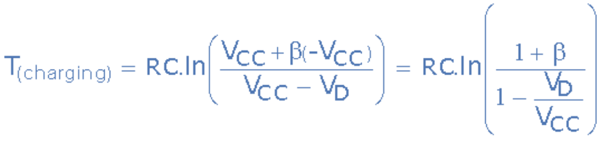
Where: Vcc is the supply voltage, V_D is the forward voltage drop of the diode (typically around 0.6 to 0.7 volts), and β is the feedback fraction.
To ensure the operational amplifier monostable circuit has a reliable negative trigger signal, which initiates the timing cycle at the rising edge of a negative pulse and prevents erroneous triggering when the circuit is stable, an RC differential circuit can be added to the input.
A differentiator circuit can be employed to generate negative output spikes based on square or rectangular input waveforms. When the comparator's threshold voltage drops sharply below its feedback fraction β, the op-amp monostable circuit enters its timing cycle. The differentiator circuit is formed using a resistor-capacitor network (as shown).
RC Differentiator Circuit Diagram:
Clearly, the capacitor requires time to recharge from -Vcc * β back to V_D (0.7V). During this period, a second negative pulse may fail to initiate a new timing cycle.
Therefore, to ensure the monostable circuit functions correctly upon the next trigger pulse, the trigger pulses must exceed the timing duration T plus the time required for the trigger pulse to charge the capacitor.(T charge).
The charging recovery time is: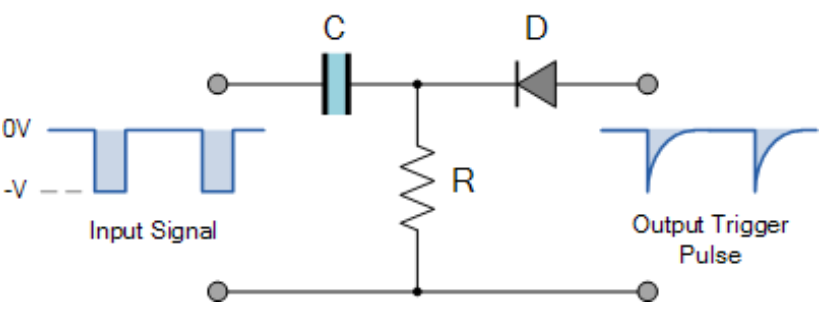
The basic differentiator circuit above uses another resistor-capacitor (RC) network, whose output voltage is the derivative of the input voltage with respect to time. When the input voltage changes from 0 to -Vcc, the capacitor begins to charge exponentially. Since the capacitor voltage Vc initially equals zero, the differentiator output voltage abruptly jumps from 0 to -Vcc, generating a negative spike that then decays exponentially as the capacitor charges.
Typically, for RC differentiator circuits, the peak magnitude of the negative spike is approximately equal to the amplitude of the trigger waveform. Similarly, as a general rule of thumb, for an RC differentiator to produce a sharp, narrow spike, the time constant (τ) should be at least ten times smaller than the input pulse width. Thus, for example, if the input pulse width is 10 ms, the 5RC time constant should be less than 1 ms (10%).
The advantage of using a differentiator circuit is that any constant DC voltage or slowly varying signal will be blocked, allowing only rapidly changing trigger pulses to initiate the monostable timing cycle. Diode D ensures that the trigger pulse reaching the operational amplifier's non-inverting input is always negative.
Adding an RC differentiator circuit to a basic operational amplifier monostable circuit yields: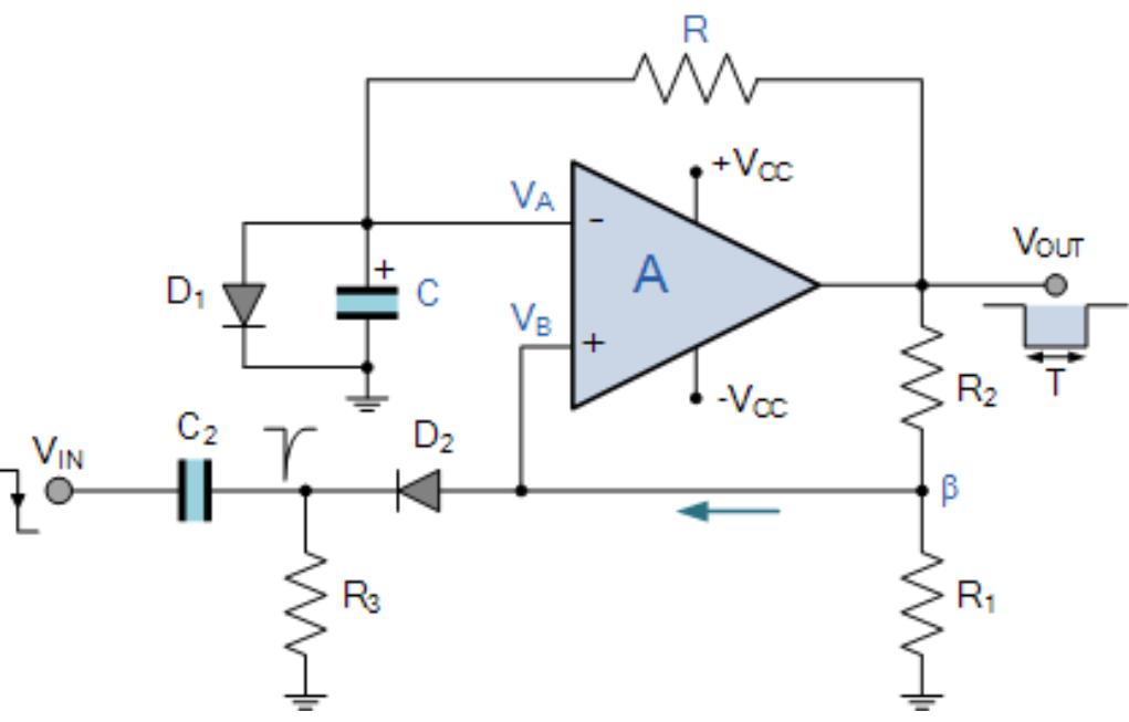
A monostable circuit using an operational amplifier is constructed with the following components: R1 = 30 kΩ, R2 = 30 kΩ, R = 150 kΩ, and C = 1.0 μF. If the op-amp is powered by ±12V to form the monostable circuit, and a 10ms pulse initiates the timing cycle,
Calculate the circuit's timing period, capacitor recovery time, total time between trigger pulses, and the value of the differentiator network. Draw the completed circuit.
Given data: R1 = R2 = 30kΩ, R = 150kΩ, C = 1.0uF, pulse width equals ten milliseconds (10ms).
Timing period T: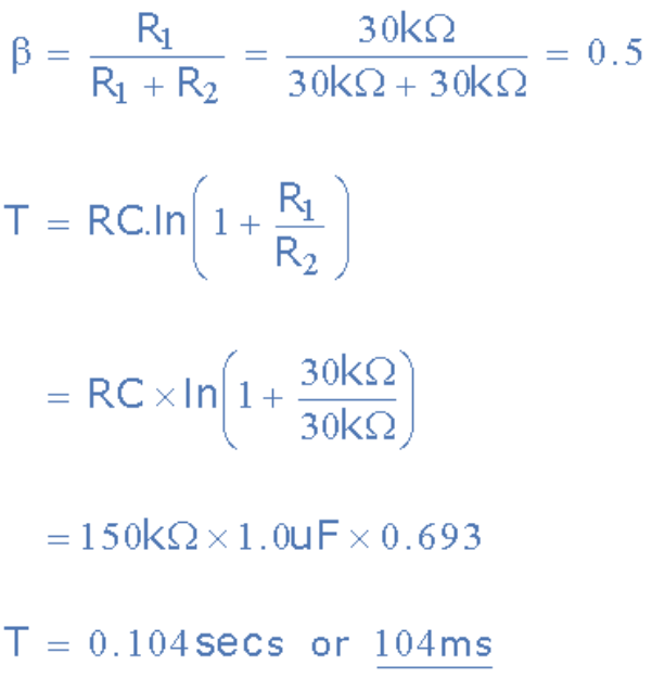
Capacitor recovery time: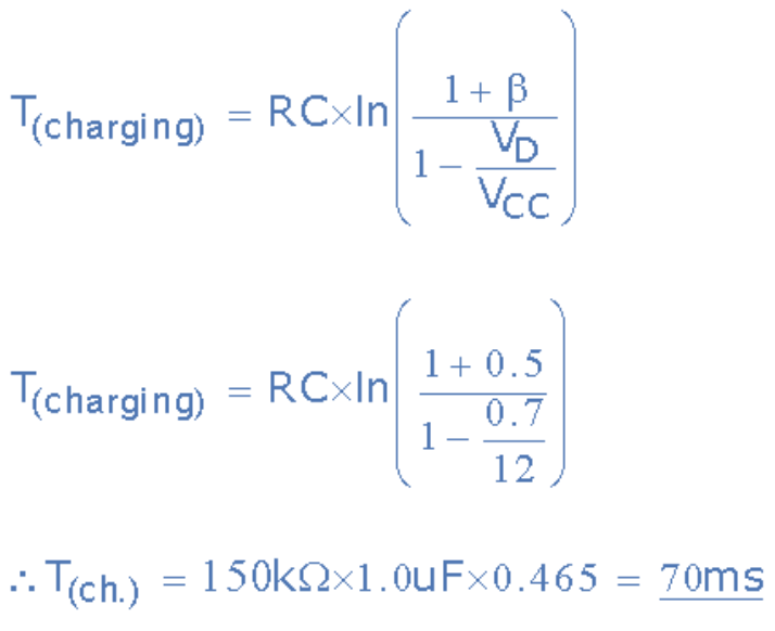
Total time between trigger pulses: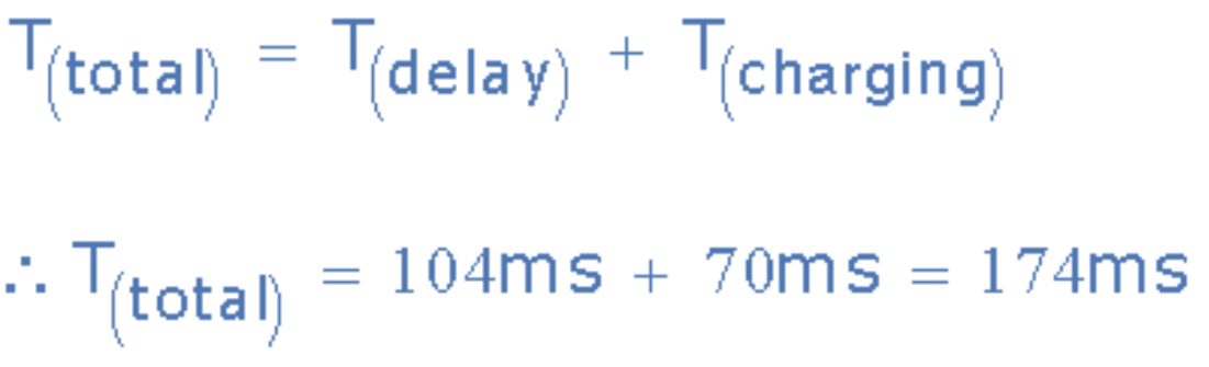
The input pulse is 10 ms, so the negative spike duration is 1 ms (10%). If we assume a capacitance value of 0.1 uF, the formula for calculating the RC value of the differentiator is: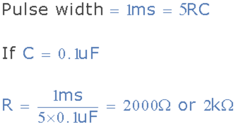
For our example, this provides the final operational amplifier monostable circuit: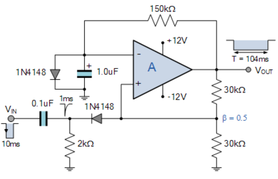
Construct a monostable circuit using a general-purpose operational amplifier (such as the 741) and several other components. While it may be easier to build monostable (single-shot) circuits using discrete components, digital logic gates, or a general-purpose 555 IC chip, there are times when an analog monostable circuit must be constructed using an op-amp.
By configuring the operational amplifier as a Schmitt trigger with positive feedback, the duration of the output pulse depends on the time constant of the RC timing circuit and the ratio value of the resistor divider network providing the positive feedback. This helps destabilize the circuit.
-
Timer Monostable Circuit
(1) Circuit Structure
- External Trigger (High Trigger Sets 0 Terminal th)
Low trigger sets terminal 1 active via capacitor C's charge/discharge, automatically returning to steady-state to generate negative pulses.
- External Trigger (Low Trigger Sets 1 Terminal tr)
High trigger sets 0 terminal to the active via capacitor C's charge/discharge, automatically returning to steady-state 0 to generate positive pulses.
ui = tr, where the collector of v is connected to VCC via resistor r and to ground via capacitor c.
r and c serve as timing elements.
(1) How It Works
- Steady State
Without external triggering, u1 is at a high level, uih; the steady state is 0, uc1 = 0, and uo = 0.
After power-on, VCC charges capacitor C through resistor R. When the voltage across capacitor C reaches at least 2/3 of VCC, uc1 = 0. Simultaneously, ui > 2/3vcc, uc2=1, q=0, q=1, output u0=0.V turns on, rapidly discharging capacitor C through V. uc≈0, uc1=1. At this point, both inputs of the basic RS flip-flop are high (1), maintaining the zero state unchanged.
- The flip-flop enters a metastable state
When u1 transitions from uih to a low level below 1/3 VCC, uc2 = 0. At this point, uc1 = 1, the basic RS flip-flop is set to 1, q = 1, and the output uo transitions abruptly from a low level to a high level, uoh. Simultaneously, transistor v turns off. Now, VCC charges C through R, and the circuit enters a metastable state. During the transient state, if the input voltage ui returns to a high level, uc2 becomes 1.
- Automatic Return to Stable State
During capacitor C charging, when uc gradually increases until uc≥vcc, uc1 becomes 0. At this point, q=0 and q=1, causing the output uo to jump from the high level uoh to the low level uol.Simultaneously, transistor V turns on, rapidly discharging C through V until UC = 0. The circuit returns to a stable state.
- Parameter Calculation
Pulse width TW denotes the duration of the transient state, representing the time required for capacitor C to charge from 0V to VCC. It can be estimated using the following formula: TW = RCLn3 ≈ 1.1RC.
Application Scenarios of Monostable Multivibrators
The monostable multivibrator, also known as a monostable circuit, is an exceptionally useful circuit in the electronic world. Its core value lies in transforming an unpredictable, chaotic input event into a clean, regular output pulse with precise duration. All its applications revolve around this fundamental characteristic.
|
Application |
Problem |
Solution |
Working Principle |
Example |
|
Pulse Shaping and Debouncing |
When mechanical switches, buttons, or relays make or break a connection, the elasticity of their metal contacts causes a series of rapid, non-ideal oscillatory transitions within milliseconds, rather than a clean switching edge. This phenomenon is known as bounce. If this signal is fed directly to digital circuits (such as microcontrollers or counters), it may be misinterpreted as multiple inputs. |
Use the jitter signal as the trigger input for the monostable circuit. |
Regardless of how chaotic or brief the trigger signal (button press) may be, the monostable circuit generates a clean, smooth rectangular pulse with a fixed width (e.g., 20ms). This pulse width is significantly longer than the jitter time, ensuring the output remains a single, definitive logic signal. |
All applications utilizing mechanical switches, such as computer keyboards, calculator buttons, and elevator buttons. |
|
Delay and Timing |
It is necessary to delay a specific amount of time after an event occurs before triggering another action. |
Trigger a monostable circuit using event signals (such as a sensor detecting an object). |
After triggering a monostable circuit, it enters its transient state (timing period T). This timing period can be utilized at its start, end, or throughout its duration to control other circuits. Delayed Activation: Use the rising edge of the monostable output pulse to activate a device (e.g., motor, light), achieving "event occurrence" followed by a "delay T" before "action."Delayed Shutdown: A device that was continuously active is turned off using the falling edge of the monostable output pulse, achieving "continuous operation for duration T" after "event occurrence" before "stopping". |
Automatic Lavatory Faucet: Hand insertion (trigger) activates water flow for 5 seconds (timed cycle T), then automatically shuts off. |
|
Timer (a direct extension of the delay function) |
A simple, low-cost timer-based on/off control is required. |
Using a monostable circuit as the core timing element |
Manual button triggers a monostable circuit, whose output directly drives the load (e.g., via a transistor or relay). |
Darkroom Timer: Press the button to illuminate the darkroom's safety light for a preset duration. Energy-Saving Light: Press the button to illuminate the hallway light for 2 minutes before it automatically turns off. |
|
Noise Cancellation and Random Pulse Detection |
In noisy electrical environments, extremely brief spike pulses (noise) may occur. We do not wish to respond to this meaningless noise, but only to valid signals that persist for a sufficiently long duration. |
Input the signal into the monostable circuit. |
Set the monostable timing period T slightly longer than the noise duration but shorter than the valid signal duration. Short noise: Triggers the monostable but outputs a pulse width of T. If no subsequent valid signal follows, the circuit produces only a T-width pulse that can be ignored by subsequent circuits.Long valid signal: The first noise or valid edge triggers the monostable, generating a pulse of width T. Since the valid signal persists, its high level will retrigger the monostable after its output ends (if circuitry permits), producing continuous pulses that indicate the valid signal's genuine presence. |
Noise Filtering in Industrial Sensor Signal Processing and Communication Lines |
Design and Experiment of Monostable Multivibrators
Taking the design of the 555 timer as an example
-
Common Circuit Design Pitfalls and Traps
Frequently Asked Questions
Common Misconceptions
Common Pitfalls
Solutions
Trigger Pulse Issue
Believe that any signal can trigger
The TRIG pin of the 555 requires a low-level pulse (voltage < 1/3 Vcc) with a sufficiently short duration (significantly less than the desired output pulse width T). An excessively long low pulse will cause the output to remain high throughout the entire low pulse period and for an additional T time, resulting in timing errors.
A simple RC differentiator circuit converts the long pulse generated by pressing the button into a short spike pulse.
RC values become extreme
Use a small resistor paired with an extremely large capacitor to achieve long timing.
Resistance values that are too low (<1 kΩ) will overload the internal discharge transistor of the 555 timer, causing it to overheat or fail. Capacitance values that are too high (> 1 μF) necessitate the use of electrolytic capacitors, which have significant leakage current. This leakage current severely compromises timing accuracy, as it effectively acts as a parallel resistance to R.
Maintain R above 10kΩ. Use tantalum capacitors or film capacitors instead of electrolytic capacitors to achieve longer and more precise timing. For extremely long timing requirements, consider using a divider such as the CD4060.
Power supply decoupling omitted
Connect Vcc and GND directly on the breadboard without any filter capacitors.
When switching output states, the 555 generates significant power supply current spikes, causing voltage fluctuations. These fluctuations may feed back to the THRES and TRIG pins, leading to unstable circuit operation or even random oscillations.
Be sure to connect a 100nF ceramic decoupling capacitor as close as possible between the Vcc and GND pins of the 555 timer. For higher-power circuits, also connect a 10μF tantalum capacitor in parallel.
Reset pin left floating
Leave RESET (pin 4) floating.
Floating pins are prone to picking up environmental noise, causing the circuit to reset unexpectedly and the output to go low prematurely.
If the reset function is not used, the RESET pin must be connected directly to Vcc.
Load connection error
Connect high-current loads (such as relays or motors) directly between the OUT pin and GND
The output pins of the 555 timer have a current limit (approximately 200mA). Directly driving high-current loads will burn out the chip.
Use the OUT pin to drive a transistor (such as a BJT or mosfet), then use the transistor to control the load. This is the standard approach.
-
Simulation and Experimental Validation
(1) Simulation
Before conducting physical experiments, performing software simulations can significantly increase success rates and deepen understanding.
Tools: LTspice, Proteus, or Multisim.
Simulation Steps:
- Build a 555 monostable circuit.
- Set up a voltage source as the trigger signal (e.g., a 5V pulse source initially high, briefly going low, then returning high).
- Run Transient Analysis with the simulation time set to 2-3 times the expected pulse width.
- Add probes to observe waveforms at key points, such as the trigger input, output, and capacitor voltage.
Verification Items:
- Does the output pulse width match the calculated value of T = 1.1RC?
- Does the capacitor voltage charge from 0V and drop when reaching ~2/3 Vcc?
- Is the trigger pulse effective?
(2) Actual Experiment
Tools: Breadboard, 555 timer IC, resistors, capacitors, LED (for visual output display), pushbutton switch, oscilloscope (essential), power supply.
Experimental Procedure:
- Wiring
Carefully verify Vcc and GND connections.
- Pre-powerup check
Use multimeter continuity setting to test for short circuits between power supply and GND.
- Oscilloscope Observation
Channel 1: Probe contacts the opposite side of the trigger button to capture the trigger signal.
Channel 2: Probe connects to the output pin (Pin 3) to observe the output pulse.
Using Single Shot mode with a set trigger level (e.g., falling edge on Channel 1) perfectly captures the entire single event.
- Measurement and Comparison
Use the oscilloscope's cursor function to measure the actual width of the output pulse and compare it with the theoretical calculated value and simulation value.
Common Experimental Phenomena and Troubleshooting:
- No Output
Check the power supply, ground, and whether the RESET pin is connected to high. Verify that the trigger signal is valid (low level).
- Output Permanently High
Possible cause: Incorrect connection of the DISCH (pin 7) circuit prevents capacitor discharge, preventing THRES from reaching 2/3 Vcc.
- Inaccurate Output Pulse Width
Typically caused by high tolerance (e.g., ±20%) capacitors (especially electrolytic capacitors) and leakage current. Replace with higher precision capacitors.
-
Performance Optimization Recommendations
(1) Improve timing accuracy
Select low-leakage capacitors: Use film capacitors (such as polypropylene CBB) or tantalum capacitors instead of aluminum electrolytic capacitors.
Select high-precision components: Use 1% precision metal film resistors and capacitors with tighter tolerances (such as 5%).
Stabilize the power supply: Use a linear regulated power supply (such as an LDO) instead of a switching power supply to provide a clean, stable voltage for the 555 timer.
(2) Achieve extremely long or extremely short timing
Ultra-short timing (nanosecond/microsecond range): Specifically designed using high-speed comparators, not the 555 timer. The 555's internal response speed is limited.
Extremely long timing (minutes/hours):
Use a small R and a large C (e.g., R = 10 MΩ, C = 470μF), but be mindful of capacitor leakage issues. Alternatively, use a small RC constant (e.g., 1 second) to drive a binary counter/divider (such as CD4020 or CD4060). The counter outputs only once every 2^N pulses received, thereby significantly extending the timing duration. This is standard practice in professional designs.
(3) Enhance interference resistance
Add a 10nF capacitor between CVOLT and ground: This stabilizes the internal comparator's reference voltage, preventing false triggers caused by power supply noise.
Shielding: In noisy environments, connect the timing RC components with shielded wiring and protect them.
Trigger signal conditioning: Adding a Schmitt trigger (such as the 74LS14) at the front end of the trigger input can significantly improve noise immunity by shaping the signal.
(4) Reduce power consumption
The standard 555 timer consumes several milliamps of current even in the idle state. For battery-powered applications, select CMOS versions such as the TLC555, LMC555, or ICM7555. Their quiescent current can be as low as tens of microamps.
During the timing period, the output is high, and the current is primarily drawn across the timing resistor R. I = Vcc / R. To reduce power consumption while meeting timing requirements, use the largest possible R and the most minor possible C whenever feasible—a larger R results in a smaller charging current.
Conclusion
A monostable multivibrator is a pulse-generating circuit with only one stable state. Its core function is to convert irregular external trigger signals into rectangular pulses with fixed width and regular waveforms. After triggering, the circuit enters a transient state and automatically resets via its RC timing element. The output pulse width is strictly determined by the formula T≈1.1·R·C (using the 555 timer as an example).
This article systematically introduces the fundamental characteristics of monostable circuits, their differences from bistable circuits, and multiple implementation methods (including transistor, op-amp, and 555 timer solutions). It also explores their extensive application scenarios, such as pulse shaping, switch debouncing, timing delays, and noise filtering. Ultimately, the article explores common pitfalls in practical design and experimentation, simulation verification methods, and performance optimization strategies, offering a solid theoretical foundation and practical guidance for engineering applications.
Monostable circuits have long transcended their role as basic timing elements. In today's highly integrated electronic systems, they continue to play critical roles. For instance, in IoT devices where sensor signals often carry noise and exhibit irregular waveforms, monostable circuits enable pulse shaping and validity checks, enhancing the reliability of MCU data processing. CMOS-based monostable circuits (such as the TLC555) function as wake-up timers in battery-powered devices, activating the central system only within specific time windows to significantly reduce overall power consumption. In distributed sensing nodes, these circuits provide localized, simple timing logic, thereby reducing the frequency of interrupts to the central processor and improving system efficiency.
Although FPGAs and microcontrollers can program any timing logic, monostable circuits retain unique advantages. Their hardware-level reliability ensures faster responses in critical systems, such as power management and reset circuits, unaffected by software runaway or crashes, delivering higher reliability. For simple delay or debounce functions, using a 555 timer or discrete components costs significantly less than an MCU, making them the preferred solution in ultra-low-cost electronics.
As applications demand higher timing accuracy, developing timing networks with lower temperature coefficients and greater stability—such as monostable designs based on silicon oscillators—will become the trend. Stable timing functions are increasingly integrated as IP blocks within complex ASICs and SoCs, providing reliable hardware timing units for system-level chips. In sectors such as automotive electronics and aerospace, monostable circuits must maintain stability across wider voltage ranges, extreme temperatures, and radiation-resistant environments—demanding stricter component selection and circuit design standards.
FAQ
-
How does a monostable work?
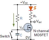
A monostable multivibrator has only one stable state (hence the name "monostable") and generates a single output pulse in response to external triggering. It returns to its initial stable state only after a time determined by the time constant of the RC-coupled circuit.
Consider the MOSFET circuit on the left. Resistor R and capacitor C form an RC timing circuit. Due to the voltage across the capacitor, the N-channel enhancement-mode MOSFET switches "ON," and the LED connected to its drain also turns "ON."
When the switch is closed, the capacitor is short-circuited and discharges, while the MOSFET's gate is grounded. Both the MOSFET and LED turn "OFF." When the switch is closed, the circuit remains in the 'OFF' state and is in an "unstable state."
When the switch opens, the fully discharged capacitor begins charging through resistor R at a rate determined by the RC time constant of the resistor-capacitor network. Once the capacitor's charging voltage reaches the lower threshold voltage level of the MOSFET gate, the MOSFET turns "ON" and illuminates the LED, restoring the circuit to a stable state.
Subsequent switching then causes the circuit to enter an unstable state, with the RC network's time constant returning it to stability after a preset timing cycle. This produces a very simple "single-triggered" or monostable multivibrator MOSFET circuit.
A monostable multivibrator, also known as a "single-shot multivibrator," generates a single output pulse of specified width—either 'high' or "low"—when triggered by an appropriate external signal or pulse T. This trigger initiates a timing cycle, causing the monostable output to change state at the cycle's start and remain in the second state.
The monostable timing cycle is determined by the time constant of the timing capacitor, C_T, and resistor, R_T, until it is reset or returns to its original (stable) state. The monostable multivibrator then indefinitely maintains this original stable state until another input pulse or trigger signal is received. Subsequently, the monostable multivibrator possesses only one stable state and undergoes a complete cycle in response to a single trigger input pulse.
-
What is the function of a multivibrator?
(1) Pulse Shaping and Debouncing
This is the most common and classic application. For instance, when mechanical switches, buttons, or relays make or break contact, the elasticity of metal contacts causes a series of rapid, non-ideal on-off oscillations to occur within milliseconds, rather than a clean transition edge. This phenomenon is called bounce. If this signal is directly fed to digital circuits (such as microcontrollers or counters), it will be mistaken for multiple inputs.
Therefore, the bouncing signal is fed into a monostable multivibrator as the trigger input for its monostable circuit. Regardless of how chaotic or brief the trigger signal (button press) may be, the monostable circuit generates a clean, smooth rectangular pulse with a fixed width (e.g., 20ms). This pulse width is significantly longer than the bouncing duration, ensuring the output is a single, definitive logic signal.
(2) Delay and Timing
Monostable circuits can generate a precise time interval by triggering the circuit with an event signal (such as a sensor detecting an object).
The principle is that after triggering the monostable circuit, it enters its transient state (timing period T). This timing period can be utilized at its start, end, or throughout its duration to control other circuits. Delayed Activation: Use the rising edge of the monostable output pulse to activate a device (e.g., motor, light), achieving "event occurrence" followed by a "delay of T" before "action". Delayed Deactivation: The device remains active initially. Use the falling edge of the monostable output pulse to deactivate it, achieving "event occurrence" followed by "continuous operation for T time" before "stopping".
(3) Timer
This is a direct extension of the delay function. Using a monostable circuit as the core timing element enables simple, low-cost timing on/off control.
Its operating principle involves a manual button triggering the monostable circuit, whose output directly drives the load (e.g., via a transistor or relay).
(4) Noise Cancellation and Random Pulse Detection
In noisy electrical environments, extremely brief spike pulses (noise) may occur. We do not want to respond to this meaningless noise, but only to valid signals that persist for a long enough time.
A monostable multivibrator can set its monostable timing period T to be slightly longer than the duration of noise but shorter than the duration of valid signals. Short noise: Triggers the monostable but outputs a pulse width of T. If no subsequent valid signal follows, the circuit produces only a single pulse of width T, which subsequent circuits can ignore. Long valid signal: The first noise or valid edge triggers the monostable, generating a pulse of width T. Since the valid signal persists, its high level will retrigger the monostable after its output ends (if circuitry permits), producing continuous pulses that indicate the genuine presence of the valid signal.
-
Why is a monostable multivibrator called so?
The following two characteristics can summarize the naming of the monostable multivibrator:
Monostable behavior: This oscillator maintains only one stable state (i.e., the initial state). After external triggering, it enters a transient state and continuously outputs pulses. Upon trigger termination, it automatically reverts to its original stable state. This behavior directly relates to the "monostable" designation.
Multiharmonic Output: Although the circuit itself lacks a steady state, through RC coupling and a deep positive feedback mechanism, the circuit state rapidly switches between two metastable states, generating a rectangular wave signal composed of multiple harmonics. This waveform is termed "multiharmonic" due to its numerous frequency components, further validating the "multivibrator" designation.
In summary, this device is named for its ability to output multiharmonic pulses in response to a single trigger continuously.
Recommended Reading:
Understanding DC Motor Components: A Comprehensive Guide
Zero-Ohm Resistor: A Comprehensive Guide to Definition, Applications, and Design Techniques