The Invisible Architects: How Dopants in Semiconductor Shape the Electrical World
Semiconductors form the bedrock of modern electronics, powering everything from smartphones and computers to solar panels and medical devices. Their unique property – an electrical conductivity that sits between that of conductors and insulators and can be precisely controlled – is what makes them indispensable. While pure (intrinsic) semiconductors like silicon (Si) or germanium (Ge) have limited usefulness, the introduction of minute, deliberate impurities, known as dopants in semiconductor, transforms them into the versatile and powerful semiconductor materials that drive our technological age. This process, doping, is the cornerstone of semiconductor device engineering, allowing us to tailor electrical properties with extraordinary precision.
The Intrinsic Foundation: Pure but Limited
In a perfect, pure semiconductor crystal (like intrinsic silicon), atoms are arranged in a regular lattice, each sharing four valence electrons with its neighbors through covalent bonds. At absolute zero temperature, all electrons are bound in these bonds, and the material acts as an insulator. As temperature rises, some extra electrons gain enough thermal energy to break free from their bonds, creating mobile negative charges (electrons) and leaving behind positively charged vacancies known as "holes." In intrinsic material, the number of free electrons (*n*) equals the number of free holes (*p*), denoted as n = p = nᵢ, where nᵢ is the intrinsic carrier concentration. For silicon at room temperature, nᵢ is very low (~1.5 x 10¹⁰ cm⁻³), resulting in relatively poor conductivity that is highly temperature-dependent.
Doping Semiconductor: Introducing Controlled Imperfections
Doping involves intentionally adding specific impurity atoms to the semiconductor lattice in very small concentrations, typically parts per million (ppm) or even parts per billion (ppb). These dopant atoms disrupt the perfect symmetry of the crystal lattice and, crucially, introduce additional energy levels within the semiconductor's band gap – the energy region between the valence band (full of bound electrons) and the conduction band (where electrons are free to move).
The genius of doping lies in selecting impurities whose atomic electronic structure differs by one valence electron from the host semiconductor atom:
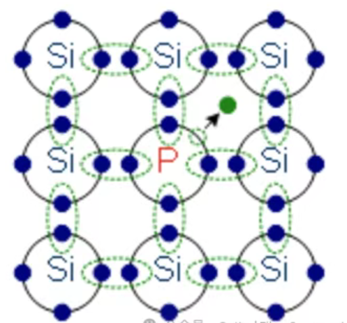
1.n-type Doping (Donors):
● Principle: Introduce atoms with five valence electrons (e.g., Phosphorus (P), Arsenic (As), Antimony (Sb)) into a group IV semiconductor (Si, Ge).
● Mechanism: The dopant atom replaces a silicon atom in the lattice. Four of its five valence electrons form covalent bonds with neighboring silicon atoms. The fifth electron is very loosely bound to the dopant atom (due to Coulombic attraction to the now positively charged dopant ion core). The energy required to free this electron into the conduction band is very small (typically a few tens of meV) – much less than the energy needed to break a covalent bond in intrinsic silicon (~1.1 eV). At room temperature, almost all these "extra" electrons are thermally excited into the conduction band, becoming free negative charge carriers.
● Effect: The semiconductor now has a significant population of free electrons (n >> p). The primary charge carriers are negative. The dopant atoms are called donors because they "donate" electrons. The material becomes n-type semiconductor. The Fermi level (a quantum mechanical concept representing the energy at which the probability of finding an electron is 50%) moves closer to the conduction band.
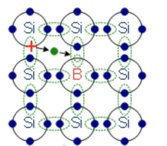
2.p-type Doping (Acceptors):
● Principle: Introduce atoms with three valence electrons (e.g., Boron (B), Aluminum (Al), Gallium (Ga)) into a group IV semiconductor.
● Mechanism: The dopant atom replaces a silicon atom. It has only three electrons to offer for covalent bonding. To complete the fourth bond, it readily "accepts" an electron from a nearby silicon-silicon bond. This creates a mobile hole (a positive charge representing the absence of an electron) where the electron was taken and leaves the dopant atom negatively charged (ionized). The energy required to promote an electron from the valence band to the acceptor level (creating a hole in the valence band) is also very small.
● Effect: The semiconductor now has a significant population of mobile holes (p >> n). The primary charge carriers are positive. The dopant atoms are called acceptors because they "accept" electrons, effectively generating holes. The material becomes p-type semiconductor. The Fermi level moves closer to the valence band.
The Power of Control: Carrier Concentration and Conductivity
The conductivity (σ) of a semiconductor is directly proportional to the concentration of free charge carriers and their mobility (μ): σ = q(nμₙ + pμₚ), where *q* is the electron charge, *n* and *p* are electron and hole concentrations, and μₙ and μₚ are their respective mobilities.
Doping provides exquisite control over *n* and *p*:
● Concentration: The free carrier concentration in doped material is approximately equal to the concentration of ionized dopant atoms at room temperature (n ≈ N_D for n-type, p ≈ N_A for p-type, where N_D and N_A are donor and acceptor concentrations). This allows conductivity to be tuned over many orders of magnitude (e.g., from intrinsic Si ~ 4 x 10⁻⁴ S/cm to heavily doped Si > 1000 S/cm).
● Type: Deciding whether electrons or holes are the majority carriers is fundamental to device design.
● Reduced Temperature Dependence: While intrinsic conductivity depends exponentially on temperature (due to thermal generation of carriers), doped semiconductor conductivity is primarily determined by the fixed dopant concentration at typical operating temperatures, making it much more stable.
Beyond Silicon: Compound Semiconductors
The doping principles extend to compound semiconductors like Gallium Arsenide (GaAs), Indium Phosphide (InP), or Gallium Nitride (GaN), which are crucial for high-speed electronics, optoelectronics (LEDs, lasers), and power devices. However, doping can be more complex:
● Site Preference: Dopants can potentially occupy different atomic sites (e.g., Ga or As sites in GaAs), affecting their electrical activity.
● Compensation: Unintentional impurities or dopants of the opposite type can "compensate" each other, reducing net carrier concentration.
● Auto-compensation & Limits: Some materials exhibit limits to achievable doping due to intrinsic defects or complex compensation mechanisms. For example, achieving high p-type doping in GaN historically was challenging (though now possible using Magnesium (Mg)).
● Alternative Dopants: Specific dopants are chosen for compatibility and activation efficiency (e.g., Silicon (Si) or Tellurium (Te) for n-type GaAs, Carbon (C) or Magnesium (Mg) for p-type GaAs).
The Engine of Modern Devices: Doping in Action
The ability to create localized regions of n-type and p-type material within a single semiconductor crystal is the foundation of virtually all semiconductor devices:
1.The p-n Junction Diode: The fundamental building block. Formed by placing p-type and n-type material in intimate contact. Creates a depletion region, enabling rectification (current flow in one direction only) – essential for power supplies, signal demodulation, and logic circuits.
2.Bipolar Junction Transistors (BJTs): Consist of alternating n-p-n or p-n-p layers. Doping levels control gain, speed, and electric current handling. Used in amplifiers and certain high-speed logic.
3.Field-Effect Transistors (FETs): The workhorses of modern integrated circuits (ICs). MOSFETs (Metal-Oxide-Semiconductor FETs) rely on creating a conductive channel between source and drain regions (heavily doped n+ or p+) by applying a voltage to the gate. The threshold voltage, transconductance, and on/off electrical current ratios are critically dependent on the doping profile in the channel and source/drain regions. Billions of precisely doped FETs form a microprocessor.
4.solar cells: Typically based on a large p-n junction. Doping creates the internal electric field that separates photo-generated electrons and holes, driving them to opposite contacts to produce electricity.
5.Light Emitting DIODES (LEDs) and Lasers: Rely on p-n junctions formed in direct bandgap semiconductors (like GaAs, InP, GaN). Electrons and holes recombine across the junction under forward bias, releasing energy as light. Doping controls carrier injection efficiency and recombination rates.
6.Sensors: Doping profiles can be tailored to change resistance or capacitance in response to light, temperature, electric fields, or specific chemicals.
Modern Challenges and Advanced Concepts
As devices shrink to nanometer scales (following Moore's Law and beyond), doping faces new frontiers and challenges:
1.Ultra-Shallow Junctions: Creating very thin, highly doped layers near the surface for advanced FETs requires precise control to avoid dopant diffusion during processing. Techniques like Rapid Thermal Annealing (RTA) and laser annealing are crucial.
2.Dopant Fluctuations: At atomic scales, the random placement of a finite number of dopant atoms within a tiny device volume leads to statistical variations in threshold voltage and performance, posing a major challenge for device uniformity and scaling.
3.Activation Limits: Getting all dopant atoms electrically active becomes harder at high concentrations due to clustering or precipitation. Novel annealing techniques and co-doping strategies are explored.
4.Doping in Novel Materials: Integrating new materials (e.g., 2D materials like graphene or transition metal dichalcogenides, high-k dielectrics, complex oxides) requires developing compatible doping techniques, often fundamentally different from traditional substitutional doping in bulk crystals.
5.δ-Doping (Delta-Doping): Creating atomically thin, extremely high-concentration doping planes within a semiconductor, enabling unique quantum effects and high electron mobility devices.
6.Precise Placement: Techniques like ion implantation followed by annealing remain dominant, but molecular beam epitaxy (MBE) allows for atomic-layer-precision doping during crystal growth.
Conclusion: The Indispensable Alchemy
Dopants, though present in minuscule quantities, are the invisible architects of the semiconductor revolution. By selectively introducing specific impurities, we perform a kind of atomic-scale alchemy, transforming the fundamental electrical character of materials like silicon and gallium arsenide. The ability to precisely control carrier type and concentration through n-type and p-type doping underpins the design and function of every transistor, diode, solar cell, and LED that powers and connects our modern world. From the simplicity of the p-n junction to the mind-boggling complexity of billion-transistor microprocessors, doping remains the essential process that breathes electronic life into semiconductor crystals. As technology pushes towards ever-smaller scales and novel materials, the science and engineering of semiconductor doping will continue to evolve, remaining absolutely central to unlocking the next generation of electronic and photonic devices. It is a testament to human ingenuity that by strategically adding imperfections, we create the perfection demanded by our digital age.