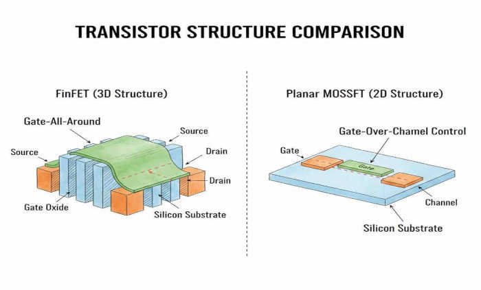
FinFET vs MOSFET: Struct, Perf, App Sel
| Table of Contents |
In the field of electronic engineering, FinFETs and MOSFETs are two core transistor device categories. The former addresses leakage issues in traditional planar MOSFETs under advanced processes through its 3D structure, while the latter remains widely used in mid-to-low performance scenarios due to its low cost and mature manufacturing processes. Understanding their differences is a fundamental basis for circuit design and device selection.
I. Key Differences at a Glance: 3-Minute Summary of Critical Distinctions
When selecting devices, engineers primarily focus on three dimensions: structural form, performance characteristics, and applicable scenarios. The table below directly compares the core differences between the two device types, helping you quickly establish a clear understanding:
|
Comparison Dimension |
FinFET (Fin Field-Effect Transistor) |
|
|
Structure |
Planar structure (2D), gate controls the channel only from above |
Fin-based 3D structure, gate wraps around the channel on three sides (similar to a "fish fin" being sandwiched) |
|
Gate Control Capability |
Single-sided control; channel current susceptible to drain-source voltage influence |
Triple-sided encapsulation provides strong control capability and significantly reduces leakage current. |
|
Process Compatibility |
Primarily mature processes (≥40nm), low cost |
Core devices in advanced processes (≤28nm), high cost |
|
Leakage rate |
Higher (especially at smaller dimensions), high static power consumption |
Extremely low, static power consumption, 1-2 orders of magnitude lower than MOSFET |
|
Switching speed |
Moderate to low speed, average performance in high-frequency scenarios |
High speed, suitable for high-frequency digital circuits |
|
Typical Applications |
Power management, motor drives, and low-voltage appliances |
CPU/GPU, high-end SoC, 5G chips, AI accelerators |
II. What Is a MOSFET?
The MOSFET is the most familiar "old friend" to electronics engineers, appearing everywhere from introductory "light-up circuits" to power modules in industrial equipment. Grasping its structure and characteristics is fundamental to understanding FinFET technology.
2.1 Structure and Working Principle: Simple Yet Practical Planar Design
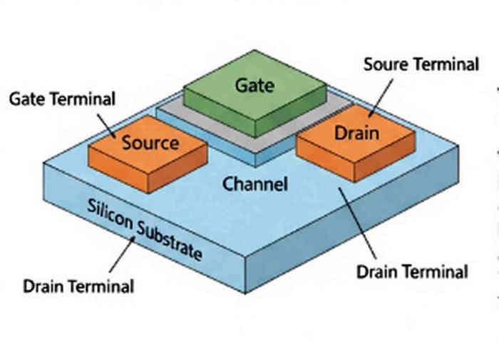
The core of a MOSFET is its "source - gate - drain" three-terminal structure. The substrate is made of semiconductor material (typically silicon). The gate is separated from the channel by a gate dielectric. Historically, silicon dioxide (SiO₂) has been used, but advanced processes increasingly adopt high-k dielectrics (e.g., HfO₂) and metal gates to reduce equivalent oxide layer thickness and enhance device performance. The overall layout is planar.
During operation, applying voltage to the gate creates an electric field that attracts charge carriers (electrons or holes) from the substrate to form a "channel," allowing current to flow from the source to the drain.
The greater the gate voltage, the wider the channel, and the higher the current — this is the core logic of "voltage controlling current."
Simply put, it functions like an "electronic valve," where the gate voltage acts as the "switch" controlling the flow and magnitude of current. The advantage of this planar structure is its simple manufacturing process and low cost. However, when dimensions shrink below 28nm, "short channel effects (SCEs)" become severe. This diminishes the gate's control over the channel, leading to increasingly noticeable "incomplete valve closure" — increased leakage current and skyrocketing static power consumption.
2.2 Advantages, Disadvantages, and Typical Applications: The Cost-Effective Choice
MOSFETs exhibit pronounced strengths and weaknesses, requiring careful trade-off analysis based on application scenarios:
- Advantages: Mature process technology (mass-produced from tens to hundreds of nanometers), low cost (typically significantly lower than comparable advanced FinFET processes, though the exact difference depends on device type, packaging, and production scale, making it difficult to generalize with a single multiplier). Excellent high-temperature tolerance (some models withstand temperatures above 150°C);
- Disadvantages: High leakage rate (particularly pronounced at small dimensions), weak drive capability (requiring multiple transistors in parallel for high-current applications).
- Typical Applications:
- Power Management: DC-DC converters, LDO regulators (e.g., MOSFETs in mobile phone chargers);
- Motor drives: Home appliance motors (washing machines, air conditioners), industrial servo motors;
- Low-voltage control: Automotive body electronics (window/door lock control), consumer electronics interface circuits.
III. What Is a FinFET?
As chip processes shrink to 28nm and below, the "leakage crisis" in planar MOSFETs becomes increasingly severe—like drafty windows that let air in even when closed. FinFETs address this by using a 3D structure to "seal the gap."
3.1 FinFET's 3D Structure and Operation
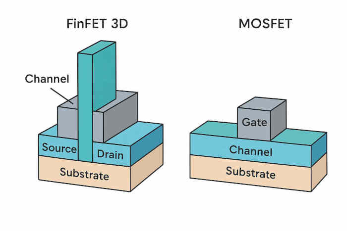
The core innovation of FinFET lies in its "fin structure" + "tri-gate" architecture:
First, a raised "fin-like" semiconductor structure (Fin) is etched onto the substrate to serve as the current channel;
The gate wraps around the Fin from the top and both sides, much like pinching a fish fin with your fingers. This three-sided gate structure significantly enhances the gate's electrostatic control over the channel, substantially reducing short-channel effects and static leakage under identical scaling conditions. The specific improvement varies depending on the process, Fin geometry, and bias conditions (typically ranging from several times to an order of magnitude better).
To illustrate: MOSFETs are like "pressing dough from above" with limited force; FinFETs are like "enclosing dough with a mold," offering superior control. This structure fundamentally resolves leakage issues at small scales, becoming the "standard configuration" for advanced processes like 7nm and 5nm.
Operating Principle: When the gate is energized, the electric field envelops the channel from three directions, providing vastly superior control compared to planar MOSFETs and significantly reducing leakage. This is equivalent to replacing the original "flat gate" with a "three-dimensional gate," enabling tighter closure and more precise control.
3.2 Advantages, Limitations, and Use Cases
FinFET excels in high-performance scenarios but entails higher costs and greater process complexity:
- Advantages: Extremely low leakage rate (low static power consumption), fast switching speed (excellent high-frequency performance), strong drive capability (single transistor supports higher current);
- Disadvantages: Complex manufacturing (requires 3D lithography and etching), high cost (design and production costs are 2-3 times that of MOSFETs), and poor cost-effectiveness in low-power applications.
Typical Application Scenarios:
- High-end chips: CPUs (e.g., Intel Core, AMD Ryzen), GPUs (NVIDIA RTX series);
- Advanced SoCs: Mobile processors (Apple A-series, Qualcomm Snapdragon 8-series);
- High-frequency communications: 5G base station chips, satellite communication devices;
- AI Computing: AI accelerators (e.g., NVIDIA A100, Huawei Ascend 910).
- Semiconductor manufacturing: Motion control modules of precision equipment such as lithography machines and wafer inspection devices — such scenarios require sinusoidal encoders to achieve nanoscale position and speed feedback, and their phase demodulation process imposes stringent requirements on signal noise suppression and dynamic response speed. Zhao et al. (IEEE Sensors Journal, 2023) proposed a phase demodulation strategy based on the Kalman filter, which points out that such sensor signal processing circuits need transistors with low parasitic capacitance and high switching speed to avoid signal distortion. The 3D gate structure of FinFETs perfectly meets this demand, and their low leakage and high-frequency characteristics can ensure the real-time performance and accuracy of the demodulation algorithm.
IV. A Comprehensive Showdown from Structure to Performance
Surface differences alone are insufficient; engineers must also consider electrical characteristics, process costs, and other details when selecting components. Below is a comparison across three core dimensions:
4.1 Structure and Gate Control: The "Fundamental Difference" Determining Performance
|
Characteristics |
MOSFET |
FinFET |
|
Channel Control Method |
Top single-gate control; channel susceptible to drain-source voltage (Vds) |
Triple-gate encapsulation minimizes Vds impact on channel, enabling more stable control |
|
Channel Length (Lg) |
Planar layout, minimum length constrained by lithography precision (≥40nm) |
3D layout, minimum length achievable below 5nm (e.g., TSMC 5nm process) |
|
Oxide layer thickness |
Thick (≥2nm), low breakdown risk |
Ultra-thin (≤1nm), requiring a more precise oxidation process |
Simply put: FinFET's 3D structure enables "stable control even at small dimensions," while MOSFETs, when scaled down, behave like "a valve that becomes increasingly loose," resulting in significantly reduced control precision.
4.2 Leakage, Power, and Speed: Performance-Level Dominance
At the 14nm process node, the performance gap between FinFET and MOSFET is starkly evident:
- Leakage current: FinFET leakage current is approximately 0.1 nA/μm, while MOSFET leakage current reaches up to 10 nA/μm—the former's static power consumption is only one-hundredth that of the latter. FinFET can deliver several times to an order-of-magnitude reduction in static leakage and significant power efficiency improvements across many advanced processes, though this cannot be generalized by a single fixed ratio.
- Switching Speed: FinFETs exhibit lower parasitic capacitance and superior electrostatic control at advanced nodes, resulting in generally faster logic switching speeds than planar CMOS. However, specific delays depend on process and design and should not be compared using fixed values—FinFETs demonstrate superior performance in high-frequency circuits (e.g., above 1GHz).
- Power Efficiency: FinFETs consume over 60% less power than MOSFETs when performing identical logic operations, which is critical for mobile devices like smartphones and laptops.
4.3 Scalability and Cost: The Trade-off Between Process and Cost-Effectiveness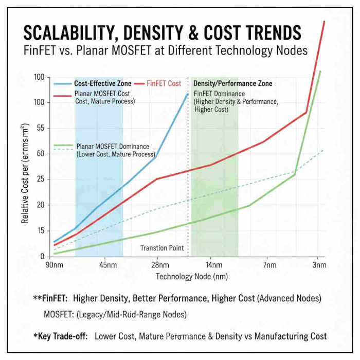
- Scalability: MOSFETs achieve stable mass production at 40nm and above, but leakage issues remain unsolved below 28nm. FinFETs have been widely adopted across many advanced logic nodes (from 22nm/16nm to 7nm, 5nm, etc.) to address scaling challenges, though alternative or complementary solutions like GAA (Gate-All-Around) have emerged at the most advanced nodes. The optimal solution chosen by different foundries varies based on their process roadmap, production capacity, and design requirements.
- Manufacturing Costs: Using the 28nm process as an example, FinFET wafer costs are approximately 1.8 times those of MOSFETs, while design costs (EDA tools, verification) can be as high as 2-3 times greater.
- Package Cost: FinFETs are typically integrated into complex IC chips using high-end packages like BGA or FCBGA. Their packaging and testing costs generally exceed those of simple discrete packages (e.g., SOT-23, TO-220), though specific cost differences depend on device complexity and production volume.
V. From Process to Device: Technology Evolution
5.1 Iteration from Planar MOSFET to FinFET
Early chips utilized planar MOSFETs. At that time, transistor dimensions were large (e.g., 90nm, 65nm), and leakage issues were not prominent, making the planar structure entirely sufficient. However, as demands for chip performance and integration grew increasingly stringent, transistors became progressively smaller. By the 28nm node, leakage from planar MOSFETs significantly impacted chip power consumption, leading to the emergence of FinFET technology.
Around 2011, Intel pioneered the 22nm FinFET process, resolving leakage challenges at small scales. Subsequently, TSMC and Samsung followed suit, making FinFET the standard for advanced processes below 28nm. Simply put, FinFET isn't a replacement for MOSFET but rather an "upgraded version" for smaller nodes, addressing the inherent limitations of planar structures.
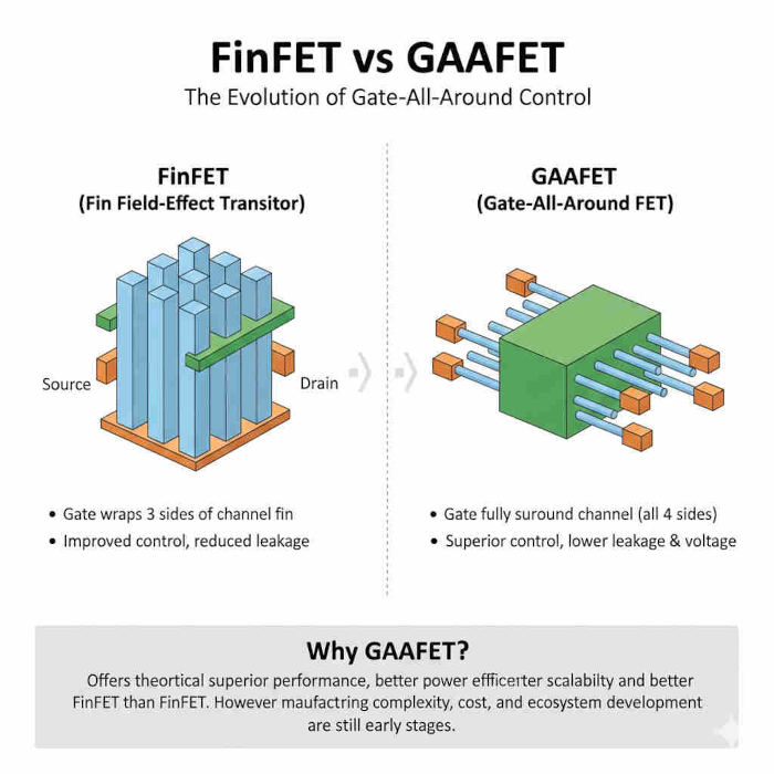
5.2 FinFET vs GAAFET: What Is the Difference?
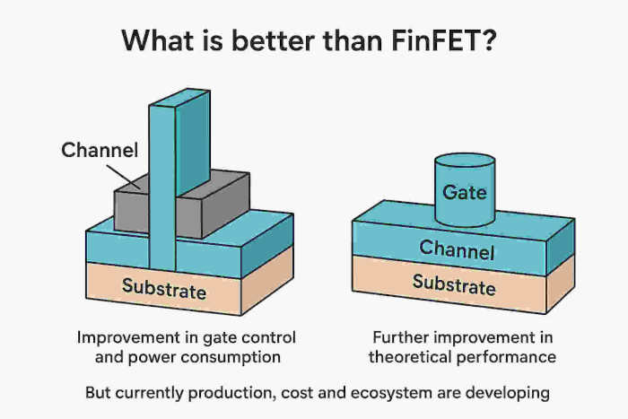
GAAFET (Gate-All-Around Field-Effect Transistor) represents a more advanced structure than FinFET. It essentially replaces the "fin-shaped channel" of FinFET with "nanowires" or "nanoplates," where the gate fully encloses the channel, enabling stronger control.
Compared to FinFET, GAAFET offers advantages including lower leakage, reduced power consumption, and better scalability. GAAFET (nanowire/nanolayer fully-integrated gate) is the mainstream solution for 2nm and future nodes—Samsung has already mass-produced GAAFET for its 3nm process, and TSMC will adopt GAAFET for its 2nm node. The term "1nm" refers to a process naming convention rather than an actual physical dimension. However, GAAFET is currently in the early stages of mass production and carries higher costs than FinFET, making it primarily suited for the most high-end chips (e.g., Samsung's 3nm mobile SoCs).
For engineers, FinFET remains sufficient for most current applications. GAAFET represents a future technology direction for the next 5-10 years; there is no urgency to adopt it now. Consideration should be postponed until the process matures and costs decrease.
VI. Comparing FET Families: jfet, MOSFET, and FinFET
6.1 JFET vs MOSFET: Which Is Better?
JFET (Junction Field-Effect Transistor) is an earlier device than MOSFET, with the core difference lying in the gate structure:
The JFET features a PN junction between the gate and channel, whereas the MOSFET employs an insulating oxide layer.
In practical applications, MOSFETs are more commonly used than JFETs for a simple reason:
- MOSFETs feature higher input impedance, simplifying drive requirements
- Lower power consumption, making it suitable for integration into chips
- They offer a wider voltage control range, making them adaptable to more scenarios
JFETs are now primarily used in specialized applications such as high-frequency small-signal amplification and low-noise circuits. MOSFETs have become the dominant choice in most consumer electronics.
6.2 Why Use a MOSFET Instead of a Transistor?
Here, "traditional transistor" refers to the BJT (Bipolar Junction Transistor). The advantages of MOSFETs over BJTs are clear:
- Requires minimal drive current and no sustained base current, resulting in lower power consumption
- High integration, enabling easy implementation in large-scale integrated circuits
- Faster switching speeds, suitable for high-frequency operation
- Simpler manufacturing processes, resulting in lower costs
Today, while BJTs are still used in some power amplifiers and analog circuits, MOSFETs are the preferred choice for most applications, including digital chips and power management ics. FinFET represents a high-end upgrade of the MOSFET.
VII. Selection Guide: FinFET or MOSFET? Application-Based Selection Guide for FinFET vs MOSFET
There is no "absolute correct" choice in selection—only "suitability." Specific recommendations are provided below by application scenario:
7.1 Supplementary Notes for Digital SoC/CPU/GPU Use Cases
The core principle for digital chip selection is "balancing performance requirements and cost"—FinFET is preferred for high-frequency, high-integration scenarios, while MOSFET offers greater advantages for low-frequency, low-cost needs. Specific correspondences are as follows:
|
Application Type |
Recommended Devices |
Reason |
|
CPU/GPU/AI Chips |
FinFET |
Requires support for high-frequency operations (typically ≥1GHz), low leakage, and integration of billions of transistors within a small area; FinFET's 3D structure is compatible with advanced 7nm-28nm processes, perfectly matching performance requirements. |
|
Low-end MCUs (e.g., 8-bit, 16-bit) |
MOSFET |
Operate at low frequencies (≤100MHz) with minimal integration requirements; MOSFETs offer lower cost while fully meeting basic control needs (e.g., simple home appliance control, sensor data acquisition). |
|
5G baseband chips |
FinFET |
Requires processing high-frequency signals ≥2GHz with stringent demands on switching speed and signal integrity; FinFET's low parasitic capacitance and low leakage characteristics minimize signal loss and ensure communication stability. |
- Supplement
These scenarios prioritize "high performance and high integration" over cost sensitivity, making FinFET the dominant choice:
Examples include mobile SoCs (e.g., Snapdragon 8 Gen series, Apple A-series), computer CPUs (e.g., Intel 12th Gen Core, AMD Ryzen series), and AI accelerator chips (e.g., NVIDIA A100). These require integrating billions or tens of billions of transistors onto a chip the size of a fingernail while ensuring high-frequency operation (≥3GHz) and low power consumption(preventing device overheating)—a requirement only met by FinFET's 3D gate structure. Traditional planar MOSFETs, with their high leakage rates and limited integration density, cannot support advanced processes below 28nm.
7.2 Supplementary Notes on Power Management and Power Electronics Applications
Core requirements for power management, motor drive, and similar applications include "high-voltage/high-current tolerance, high reliability, and low cost." Due to their structural characteristics, traditional planar MOSFETs (and their SiC MOSFET derivatives) are better suited than FinFETs for these needs. Specific selection guidelines are as follows:
- DC-DC Converters: For low-to-medium voltage applications (≤48V, e.g., mobile phone chargers, laptop power supplies), prioritize conventional MOSFETs (e.g., synchronous rectifier MOSFETs) due to their low cost and sufficient conversion efficiency. High-voltage applications (≥100V, e.g., industrial power supplies, EV high-voltage distribution) should use SiC MOSFETs. Their high-voltage and high-temperature tolerance (withstanding voltages above 1200V) reduces thermal management module size and enhances system reliability.
- Motor Drives: Industrial motors (e.g., assembly line motors) and home appliance motors (e.g., air conditioner compressors, washing machine motors) primarily use MOSFETs (typically power MOSFETs in TO-220 or TO-247 packages). Their planar structure handles high currents (tens to hundreds of amperes) at 1/3 to 1/2 the cost of equivalent FinFETs, while offering lower failure rates that meet industrial applications' longevity requirements.
- Fast Chargers: In low-voltage, high-current scenarios (e.g., 20V/10A, 100W fast charging), MOSFETs offer significantly better cost-performance than FinFETs—meeting high-frequency switching requirements (≤1MHz) without the advanced process costs of FinFETs. Current mainstream fast-charging solutions (e.g., Huawei SuperCharge, Xiaomi Surge Fast Charge) all use MOSFETs as core switching devices.
- Supplement
The core trade-off in these scenarios is "voltage/current endurance capability" versus "cost control." FinFETs suffer from structural limitations (3D gates are more susceptible to breakdown under high voltage), resulting in insufficient reliability and high process costs in high-voltage, high-current applications. Consequently, they struggle to replace MOSFETs in scenarios like industrial inverters and low-voltage auxiliary power supplies in electric vehicles (12V/24V systems), which require devices to operate stably across a wide temperature range of -40°C to 125°C. MOSFETs' planar structure enables enhanced voltage tolerance through thicker oxide layers, while mature 40nm and 28nm processes effectively control costs, fully meeting most power management requirements (conversion efficiency ≥90%).
7.3 Automotive and Industrial Control Applications
Automotive electronics demand extremely high reliability and a wide temperature range (-40°C to 150°C), with significant performance variations across different subsystems. Component selection must be tailored to specific scenarios:
- Autonomous driving chips (e.g., Orin, Mobileye EyeQ): Select FinFET (28nm-7nm process)— These chips process massive real-time data from LiDAR and cameras (tens of GB per second), demanding high computing power (TOPS-level) and low power consumption. FinFET's high integration (supporting multiple modules like GPU, NPU, ISP) and low leakage characteristics enable high-performance computing within limited vehicle space while reducing heat generation.
- Body Control (Windows, Lights): Select MOSFET (40nm-90nm process) — These scenarios require only simple switching control at low frequencies (≤50MHz) with no computational demands. MOSFETs offer low cost, strong anti-interference capabilities, and mature processes that ensure automotive-grade reliability (lifespan ≥10 years / 200,000 km), making them the optimal cost-performance solution.
- New Energy Vehicle OBC (On-Board Charger): Circuit-specific selection — High-voltage main circuits (e.g., 380V AC to high-voltage DC conversion) must withstand high voltages (≥750V). Select SiC MOSFETs, whose high-temperature tolerance and low conduction losses enhance charging efficiency (≥96%) and reduce thermal management module size. For low-voltage auxiliary circuits (e.g., 12V control circuits), standard MOSFETs suffice to meet basic switching requirements, lowering overall costs.
- Supplement:
-
- Requires processing complex algorithms or high-frequency data. Select 22nm/14nm FinFET to ensure computational power and response speedStandard industrial control modules (e.g., sensor signal amplification, relay drivers): Low performance
- requirements warrant 40nm/55nm MOSFETs, balancing cost and reliability (adapted to industrial environments with dust and vibration).
VIII. Comparing FinFET and MOSFET by Electrical Parameters
8.1 On-Resistance, Gate Charge, and Switching Loss
- On-Resistance (Rdson): The on-resistance (Rds(on)) of power MOSFETs depends on vertical structure and die area, while FinFET on-resistance is determined by fin count, width, and process node. Their operating voltage levels and applications differ significantly; no "equivalent voltage level" exists for direct Rds(on) comparison. MOSFETs are better suited for high-current scenarios; FinFETs exhibit slightly higher on-resistance but lower switching losses.
- Gate charge (Qg): FinFETs have lower gate charge than MOSFETs, enabling faster switching speeds and offering clear advantages at high frequencies.
- Switching Losses: FinFET switching losses are 30%-50% lower than MOSFETs, resulting in greater power savings in high-frequency applications (e.g., MHz-level power supplies).
8.2 Operating Voltage, Frequency, and Thermal Performance
- Operating Voltage: MOSFETs support higher operating voltages (up to 1000V+). FinFETs, used in advanced logic chips (CPUs/GPUs/SoCs, etc.), typically operate at internal supply voltages of 0.7–1.2V. This reflects system design requirements, not device voltage limitations. FinFETs are not "≤5V-specific devices" but represent a structural evolution of digital logic CMOS technology nodes.
- Operating Frequency: FinFET supports higher operating frequencies (up to GHz levels), while MOSFET exhibits slightly weaker high-frequency performance, making it suitable for MHz-level applications.
- Thermal Performance: MOSFET planar structures dissipate heat more effectively, making them suitable for high-power scenarios. FinFET thermal characteristics depend on overall chip layout, metal layer stacking, and heat dissipation paths. Heat generation primarily stems from high-density logic switching, with no straightforward causal relationship between 3D structure and "poor thermal performance." Overall, thermal management pressure is manageable.
- Practical advice for engineers: Select devices based on voltage and frequency — choose MOSFETs for high-voltage, high-current applications; opt for FinFETs for low-voltage, high-frequency scenarios.
IX. From IC Design to Component Sourcing: Practical Selection Techniques (Unikeyic Differentiation)
9.1 Typical Devices and Packages for Different Technologies
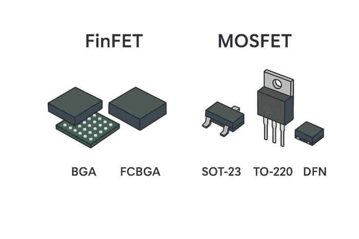
- FinFET Devices: Primarily high-end IC chips, predominantly packaged in BGA or FCBGA formats. Examples include mobile SoCs using FCBGA and FPGAs using BGA. Characterized by high pin counts and integration density.
- MOSFET Devices: Categorized into signal MOSFETs and power MOSFETs. Common packages include SOT-23, SOT-223, TO-220, and DFN. SOT-23 is suitable for small-signal applications, while TO-220 is ideal for high-power scenarios.
9.2 Supply Chain and Brand Selection
As an electronic component distributor, Unikeyic maintains over 200,000 in-stock components and partners with leading brands including NXP, TI, ST, Microchip, ADI, ON, and others. Whether sourcing MOSFETs or FinFET-related devices, reliable supply chains are readily available.
Procurement Recommendations:
- Selecting MOSFETs: Prioritize power MOSFETs from TI, ON, and ST for consistent quality and mature supply chains.
- Selecting FinFET-related ICs: Prioritize chips manufactured by Intel or TSMC, such as products from Qualcomm, Apple, and AMD, for guaranteed performance and reliability.
9.3 Stocking Strategies Across Product Lifecycles
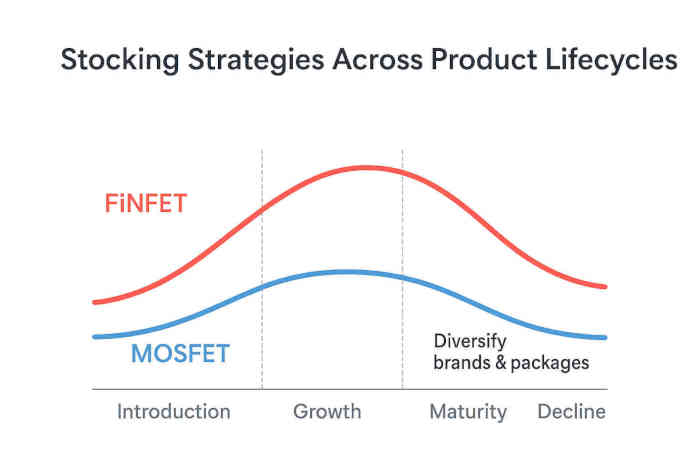
- FinFET Devices: With rapid technological iteration, older devices face discontinuation upon new releases. Stock only as needed to avoid excessive inventory and losses from obsolescence.
- MOSFET Devices: With mature technology and extended lifecycles (typically 5-10 years), moderate stocking is feasible—especially for commonly used models—to prevent production disruptions from shortages.
- Shortage Response: For popular FinFET chip shortages, contact Unikeyic engineers to explore alternative models. MOSFET shortages are less common, with most models restocked quickly.
X. Frequently Asked Questions
What is better than FinFET?
Currently, GAAFET (Gate-All-Around Field-Effect Transistor) holds greater advantages over FinFET, particularly the nanolayer structure. It enables more precise current control, reduces leakage, and is compatible with advanced processes at 3nm and below. However, GAAFET currently has a limited mass production scale and higher costs compared to mature FinFET technology, preventing its widespread replacement.
What is the difference between FinFET, MOSFET, and GAAFET?
|
Type |
Structure |
Gate Control Method |
Typical Node |
|
MOSFET |
Planar / 3D structure, source and drain on the same plane |
A single gate controls the channel from above |
90nm and above mature processes |
|
FinFET |
Fin-shaped vertical structure, source and drain form "fins." |
Triple gate (side + top) encapsulates the channel |
22nm–7nm process nodes |
|
GAAFET |
Nanowire/nanolayer structure, source and drain surround the channel |
The gate fully surrounds the channel |
3nm and below advanced process nodes |
Which is better, JFET or MOSFET?
There is no absolute "better"—it depends on the application: MOSFETs feature extremely high input impedance and low power consumption, making them suitable for digital circuits and power management requiring low static current; JFETs exhibit lower noise and better linearity, making them more suitable for applications demanding high signal quality, such as RF amplification and analog signal processing.
Why use a MOSFET instead of a transistor?
Here, "transistor" typically refers to a traditional BJT (Bipolar Junction Transistor). MOSFETs control current with voltage, eliminating the need for input current and resulting in significantly lower power consumption than BJTs. This makes them more suitable for large-scale integration (e.g., chips). Additionally, MOSFETs offer fast switching speeds and compact size, enabling adaptation to high-density circuit designs and meeting the miniaturization and low-power demands of modern electronic devices.