What is GND in Electronic Circuit?
1. Definition and Basic Concepts of GND
1.1 What is GND in Electronic Circuit?
GND, short for Ground, is a crucial concept and connection point in circuits. It is not the 'earth' but a manually defined zero-potential reference point that provides a common reference potential for all signals in a circuit, playing an indispensable role: Serving as the reference zero point (0V) for measuring all voltages in a circuit, it defines the potential of signals and serves as the reference for measuring voltages at other points in the circuit;It provides a low-impedance return path for current, forming a closed loop to ensure energy transmission. This safeguard ensures signal integrity and personal safety by diverting noise, shielding interference, and discharging static electricity.
When current flows from the positive terminal of the power source through the load, it must return to the negative terminal of the power source. This return path is typically achieved through GND. Therefore, GND is not only the return path for current but also a critical component for maintaining the regular operation of the entire circuit.
1.2 GND is not the same as 'Earth Ground'
Although it is called 'ground', it does not refer to the natural Earth (also known as Earth Ground). GND is a reference point set for circuit design and application, i.e., a point relative to the 0 level, and it is conceptually different from the natural Earth.
In specific special applications, such as for safety protection, preventing static electricity buildup, or improving circuit interference resistance, GND may need to be connected to the Earth. However, in some portable electronic devices, GND may not be directly connected to the Ground but rather serve as a 'logical ground' or 'system ground' within the circuit. Even so, it can still function as a practical reference point for the circuit.
1.3 Common Symbols for GND
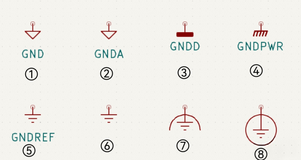
Among these:
① is the standard ground symbol
② is the analog ground symbol. It is typically used as the reference ground for analog inputs in analog-to-digital (A/D) converters. Note that although the symbol is the same as the standard GND, the network tag name is different, so they are not connected by default.
③ is the digital ground symbol, typically used on the other side of an A/D converter to provide a reference ground for digital outputs.
④ is the power ground symbol, used in circuits to indicate the local reference potential. It is typically the grounding of the metal enclosure housing the circuit, indicating that there may be a significant potential difference between the chassis ground and the true Ground.
⑤ and ⑥ are reference grounds or true Grounds, typically representing the building's 0-voltage. If this symbol is used in a schematic diagram, it indicates that this point must be directly connected to a physical metal plate that is connected to the actual Earth (Ground).
⑦ is clean Ground. In this sense, it is a specially designed 'ground' that is not affected by noise, ensuring the regular operation of sensitive equipment.
⑧ is protective grounding. This symbol represents terminals designated to prevent external shocks in the event of a system failure. Protective grounding is intended to protect (e.g., from the risk of electric shock due to insulation failure) rather than the items connected to this terminal.
2. Core Functions and Roles of GND
2.1 As a Voltage Reference Point
GND provides a common, typically zero-potential reference point for measuring the voltage of all other points in a circuit. Without this reference point, discussing the voltage of a particular point in volts would be meaningless.
2.2 Forming a Current Return Path
Current requires a complete loop to flow, and GND typically serves as the final destination (or starting point) of this loop, providing a low-impedance path for current to return to the power source's negative terminal.
2.3 Ensuring Voltage Stability and Signal Integrity
As the zero-potential reference point (0V reference point) of the circuit, all voltage measurements and signal transmissions are referenced to GND. Independent grounding systems for different functional circuits ensure signal isolation and prevent interference.
2.4 Provide safety protection
In AC power systems, the equipment housing is connected to Earth (also known as Earth Ground), with the primary function being safety. When an internal fault occurs (such as insulation failure causing a live wire to come into contact with the housing), current flows through the ground wire into the Earth, triggering a fuse or ground fault circuit interrupter to trip and cut off the power supply, preventing electric shock when someone touches the housing.
2.5 Reducing Signal Crosstalk and Electromagnetic Radiation
The shielding layer of cables is connected to GND, which can absorb or redirect external electromagnetic interference signals to prevent them from entering signal lines and interfering with sound signals. Noise generated within the circuit (such as power supply ripple or switching noise) can be absorbed or bypassed through components like capacitors connected to GND, reducing their impact on signal quality.
In multi-layer circuit boards, a dedicated GND layer is typically present, providing a stable reference plane and low-impedance return path for signal lines, thereby reducing signal crosstalk and electromagnetic radiation.
3. Types and Applications of GND
3.1 Earth Ground
The safe voltage for the human body is below 36V. If a voltage exceeding 36V is applied to the human body, it can cause injury. This is a fundamental safety consideration for engineers when developing and designing circuit projects.
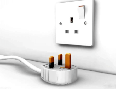
To enhance circuit safety, engineers typically use the earth ground (EGND) in high-voltage, high-current projects. For example, in household appliances such as electric fans, refrigerators, and televisions, sockets with earth ground (EGND) protection are installed.
As shown in the figure below, the socket for household appliances has three terminals. Two terminals are for the 220V live wire and neutral wire, while the third terminal serves as the protective earth ground (EGND).
Earth Ground (EGND) is connected to the Earth and serves a high-voltage protection function to ensure equipment safety. It does not participate in the project's circuit functionality and is unrelated to circuit functions.
Therefore, Earth Ground (EGND) has a distinct circuit significance difference from other types of ground lines (GND).
3.2 Chassis Ground
Chassis Ground is a special and critical type of grounding in electronic devices and electrical systems, explicitly referring to the grounding connection of the metal housing or frame of the device. Its core function is safety protection and electromagnetic compatibility (EMC).
The chassis is the metal outer casing of electrical equipment, typically grounded to ensure safety. If a person accidentally comes into contact with the metal casing of a live electrical device, the person and the device are effectively connected in parallel. Since the impedance of the metal casing is much greater than that of the human body, most of the current flows from the metal casing into the Ground, with only a small amount passing through the body, thereby preventing electric shock.
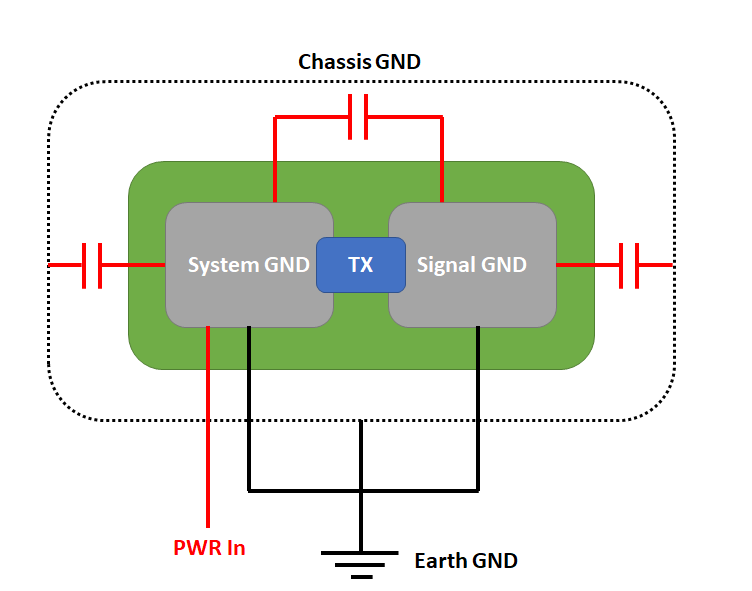
3.3 Signal Ground
Signal ground refers to the ground node used to connect signal loops. Signal ground is the ground wire used to connect all signal lines. It serves as the reference point for signal levels in a circuit, stabilizing signal levels and preventing signal noise and interference.
Signal ground is used in both analog and digital circuits to reference the ground potential. It ensures that all components use the same signal reference, thereby maintaining signal accuracy. It is commonly used in circuits sensitive to signals, such as audio amplifiers.
3.4 Analog Ground vs. Digital Ground
Analog ground (AGND) is primarily used in analog circuit sections, such as analog sensor ADC acquisition circuits and operational amplifier circuits. In these analog circuits, since the signals are analog and weak, they are easily affected by high currents from other circuits. If not distinguished, high currents can cause significant voltage drops in analog circuits, leading to signal distortion and potentially causing the analog circuit to malfunction.
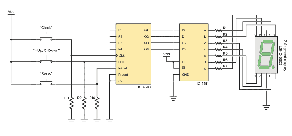
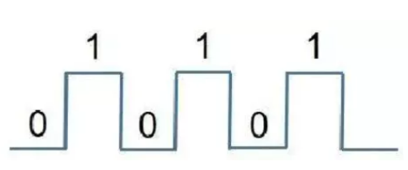
Digital Ground (DGND) is relative to Analog Ground (AGND) and is primarily used in digital circuit components, such as button detection circuits, USB communication circuits, and microcontroller circuits. The reason for establishing a digital ground line (DGND) is that digital circuits share a common characteristic: they are discrete switch signals that only distinguish between digital '0' and digital '1', as shown in the figure below.
3.5 Power Ground
The power ground is the ground connection point related to the power supply in a circuit. It is used to connect the positive terminal of the power supply voltage or the power supply location to ensure that the circuit functions properly.
Power Ground is typically connected to the negative terminal of the power supply voltage or the power supply ground to form a closed circuit, allowing current to flow normally. Power Ground also ensures the stability and safety of the power supply, preventing unnecessary current loops in the circuit. It is commonly found in power modules and motor drivers.
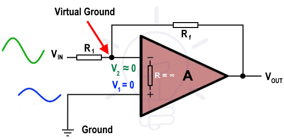
3.6 Virtual Ground
A virtual ground is a node in a circuit that maintains a constant reference potential, even though it is not directly connected to the 'real ground' reference potential. In some cases, the reference potential is considered to be the ground end of the circuit, so the aforementioned node is also referred to as a 'virtual ground'.
Similar to the 'false zero point' commonly found in operational amplifiers, it is not directly connected to Ground but has the same potential as the zero point, which is controlled by feedback. Therefore, virtual Ground is frequently used in analog circuit design and amplifier analysis.
4. Grounding Design Principles and Wiring Techniques
4.1 Star Grounding
The theoretical basis of 'star' grounding is that there is always one point in a circuit that serves as the reference point for all voltages, known as the 'star grounding' point. We can better understand this concept through an analogy: multiple conductors radiate outward from a common grounding point, much like the spokes of a star. The star point does not necessarily resemble a star in appearance—it could be a point on the grounding layer—but a key characteristic of a star grounding system is that all voltages are measured relative to a specific point on the grounding network, rather than relative to an undefined 'ground'. (Regardless of where the probe is placed.)
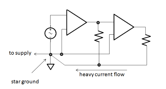
Although theoretically very reasonable, the star grounding principle is difficult to implement in practice. For example, if a system uses a star grounding design and all signal paths are drawn to minimize interference between signals and avoid high-impedance signals or ground paths as much as possible, implementation issues arise. When power sources are added to a circuit diagram, they introduce unwanted ground paths or cause significant power currents to flow into existing ground paths, which can disrupt signal transmission.
Providing separate power supplies for different parts of the circuit (and thus separate ground loops) typically resolves this issue. For example, in mixed-signal applications, analog power supplies are typically separated from digital power supplies, and the analog Ground and digital Ground are also connected at the star point.
4.2 Separating Analog Ground from Digital Ground
Digital circuits generate noise. Saturated logic (such as TTL and CMOS) draws large currents from the power supply during switching. However, since the noise immunity of logic levels can reach hundreds of millivolts or more, the requirements for power decoupling are generally not very stringent. In contrast, analog circuits are highly susceptible to noise—including noise on power rails and ground rails—so to prevent digital noise from affecting analog performance, analog circuits should be separated from digital circuits. This separation involves separating ground loops and power rails, which can be challenging for mixed-signal systems.
However, for high-precision mixed-signal systems to achieve optimal performance, it is critical to have separate analog Ground and digital Ground as well as separate power supplies. Although some analog circuits operate on a +5 V single power supply, this does not mean that the circuit can share the same +5 V high-noise power supply with microprocessors, dynamic RAM, fans, or other high-current devices. The analog portion must utilize a power supply of sufficient power to operate at peak performance, not just to remain operational. This distinction necessitates careful attention to power rails and ground interfaces.
Note that the analog Ground and digital Ground in the system must be connected at some point so that all signals reference the same potential. This star point (also known as the analog/digital common point) must be carefully selected to ensure that digital currents do not flow into the analog portion of the system. Setting the common point at the power supply location is typically convenient.
Many ADCs and DACs have separate 'analog ground' (AGND) and 'digital ground' (DGND) pins. In the device data sheet, it is typically recommended that users connect these pins at the device package. This appears to conflict with the recommendation to connect the analog Ground and digital Ground at the power supply. If the system has multiple converters, this recommendation seems to conflict with the requirement to connect the analog Ground and digital Ground at a single point.
There is no conflict. The 'analog ground ' and 'digital ground' labels on these pins refer to the internal parts of the converter to which the pins are connected, not the system ground to which the pins must be connected. For ADCs, these two pins should typically be connected and then connected to the system's analog Ground. Since the analog portion of the converter cannot withstand the voltage drop caused by digital current flowing through the wires to the chip, the two cannot be connected internally within the IC package. However, they can be connected externally.
The figure below illustrates the concept of ground connections for an ADC. This pin configuration reduces the converter's digital noise immunity by an amount equal to the common-mode noise between the system's digital Ground and analog Ground. However, since digital noise immunity is often in the hundreds or thousands of millivolts, this is generally not a significant issue.
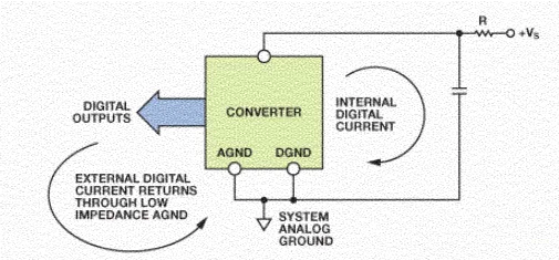
Analog noise immunity is only reduced by external digital currents flowing into the analog Ground from the converter itself. These currents should be kept very small, and can be minimized by ensuring that the converter output does not have high loads. A good way to achieve this is to use a low-input-current buffer at the ADC output, such as a CMOS buffer-register IC.
Suppose the converter's logic power supply is isolated using a small resistor and decoupled to the analog Ground via a 0.1 μF (100 nF) capacitor. In that case, all fast-edging digital currents from the converter will flow back to Ground through the capacitor and will not appear in the external ground circuit. Suppose the analog Ground is kept at a low impedance and the analog performance is adequately ensured. In that case, the additional noise generated by external digital ground currents will not pose a significant issue.
4.3 PCB Ground Plane Design
In actual engineering, connecting these different types of Ground is a critical issue. Common connection strategies include single-point grounding, multi-point grounding, and mixed grounding.
(1) Single-Point Grounding
Single-point grounding is typically used in low-frequency circuits, where all grounds are connected to the power ground through a single point. This method effectively reduces voltage differences in ground loops and avoids low-frequency noise interference. Single-point grounding is suitable for systems where analog and digital circuits are separated, typically by connecting the analog Ground and digital Ground at the power input or central ground plane. However, in high-frequency circuits, single-point grounding may introduce unnecessary parasitic inductance, preventing high-frequency signals from being effectively conducted and thereby affecting signal integrity.
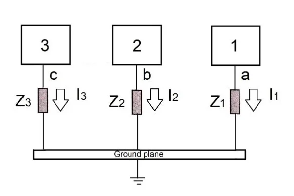
(2) Multi-point grounding
Multi-point grounding is suitable for high-frequency circuits. In this strategy, various grounds are directly connected through the ground plane. Since high-frequency signals are mainly coupled through capacitance, this method can reduce ground loop inductance and improve high-frequency signal transmission. It is worth noting that in multi-point grounding, the design of the ground plane is crucial. Poorly designed ground planes may cause noise coupling between different grounds, thereby affecting circuit performance.
(3) Mixed grounding
Mixed grounding combines the advantages of single-point grounding and multi-point grounding, offering a more comprehensive approach. Single-point grounding is used in the low-frequency portion, while multi-point grounding is used in the high-frequency portion. This method is prevalent in complex circuit designs, especially in systems that simultaneously include analog, digital, and RF circuits.
In actual PCB ground plane design, the following points require special attention during ground design:
(1) Ground plane continuity
Maintaining ground plane continuity is critical for ensuring low impedance and reducing EMI. Any discontinuity in the ground plane may cause signal reflection or interference, so cuts or interruptions in the ground plane should be avoided during design.
(2) Ground loop control
Minimizing ground loop area can reduce electromagnetic radiation. The size of the ground loop directly affects the degree of noise coupling; therefore, the loop area should be carefully controlled during routing, especially around high-speed signal lines and high-current paths.
(3) Separation of routing and Ground
When designing mixed-signal circuits, it is essential to keep digital circuits and analog circuits separate from each other. Digital signal lines should not cross analog ground planes to prevent digital noise from being introduced into the analog section. Additionally, ensure a complete ground plane at signal crossings to avoid signal integrity issues.
(4) Layer Planning
In multi-layer PCB designs, different types of ground planes can be placed on separate layers and connected via vias as needed. This effectively isolates interference between different ground planes and reduces ground plane inductance and parasitic effects through proper layer stacking.
4.4 Grounding Impedance Control
The importance of grounding impedance lies in its impact on the safety of electrical systems and the regular operation of equipment. Methods for controlling grounding impedance involve multiple aspects, including soil resistivity, grounding system design, material selection, and construction techniques.
(1) Soil Improvement
l Soil Replacement Method: Replace the original soil with soil of lower resistivity, such as clay, peat, black soil, or sandy clay. The replacement area is generally within 0.5 to 1 meter around the grounding electrode and at one-third of the grounding electrode's depth. However, this method requires a significant amount of workforce and labor hours.
l Artificial soil treatment: Adding chemicals such as salt, charcoal, furnace ash, nitrogen fertilizer residue, calcium carbide residue, and lime to the soil around the grounding electrode to enhance the conductivity of the soil surrounding the grounding electrode. Salt is practical and cost-effective, but this method reduces the stability of the grounding electrode, accelerates corrosion, and as the salt gradually dissolves and leaches away, the grounding resistance increases over time. Typically, reprocessing is required approximately two years after manual treatment has been completed.
(2) Grounding Electrode Installation
l Deep-buried grounding electrodes: When the soil or water at a deep underground location has low resistivity, deep-buried grounding electrodes can be used to reduce ground resistance. This method is most effective in sandy soils. Grounding electrodes are typically made of round steel, with lengths generally ranging from 5 to 10 meters depending on geological conditions.
l Multiple external grounding electrodes: If there are rivers or lakes with good conductivity and no freezing nearby, this method can be used. However, the length of the external grounding electrodes should not exceed 100 meters. During design and installation, the impact of the resistance of the primary grounding electrode connection must be taken into account.
l Extending horizontal grounding electrodes: As the length of horizontal grounding electrodes increases, the influence of inductance and the impact factor also increase. However, within a specific range, grounding resistance can still be reduced. Generally, the effective length of horizontal grounding electrodes should not exceed the value determined based on soil resistivity.
(3) Utilize resistance-reducing materials and special grounding electrodes
l Use resistance-reducing agents: After laying resistance-reducing agents around the grounding electrode, the external dimensions of the grounding electrode can be increased, reducing the contact resistance with the surrounding medium, thereby lowering the grounding resistance of the grounding electrode to some extent. This method is particularly effective for small-area concentrated grounding and small grounding networks.
l Using conductive concrete: Carbon fiber is added to cement as a grounding electrode. For example, adding approximately 100 kilograms of carbon fiber to 1 cubic meter of cement can form a hemispherical grounding electrode, with its power frequency grounding resistance typically reduced by about 30%. Additionally, needle-shaped grounding electrodes can be embedded in the conductive concrete further to reduce the impact of the grounding resistance value.
l Non-metallic grounding electrodes: These are made from non-metallic materials with excellent conductivity, which are composite materials formed through casting or mechanical molding, and can be used as grounding electrodes.
(4) Other measures
l Deep grounding technology: In urban areas, the deeper the soil, the lower the resistivity and the higher the moisture content. Therefore, deep grounding technology can be used to directly drive vertical grounding electrodes into the Ground, particularly suitable for areas with dense buildings or narrow grounding network zones.
l Wastewater introduction: To reduce the soil resistivity around the grounding electrode, wastewater can be directed to the area where the grounding electrode is buried. The grounding electrode is made of steel pipe, with small holes (5 mm in diameter) drilled every 20 cm along the pipe to allow water to seep into the soil.
l Deep well grounding: When conditions permit, deep well grounding can be used. A drill is used to bore a hole, and steel pipe grounding electrodes are driven into the well bore. Mud is then injected into the steel pipe and the well. Deep well grounding electrodes primarily improve the efficiency of reducing grounding resistance by increasing the length of the grounding electrode, utilizing the lower resistivity of deeper soil layers, and creating a low-resistance material-filled zone around the grounding electrode.
l Blasting fracture pressure grouting method: In rocky areas, the blasting fracture pressure grouting method can be used to reduce ground resistance. By blasting to create fractures, grounding electrodes are installed in the cracks. Then a resistance-reducing agent slurry is pressurized into the fractures using pressure machinery, thereby altering the electrical conductivity of a larger soil area to reduce ground resistance.
4.5 Avoiding ground loops and multiple grounding misconceptions
Avoiding ground loops and multiple grounding points is critical in electronic system design to ensure signal integrity, reduce noise, and prevent interference.
A ground loop refers to the presence of multiple grounding points in a system, with potential differences between these points. These potential differences drive current to flow through the ground loop, causing voltage drops along the signal path as it passes through signal ground lines or shielding layers, which interfere with the sound signal.
Common mistakes include assuming that "grounding is sufficient," ignoring potential differences between different grounding points, or grounding both ends of long-distance connections to the Earth, or grounding both ends of shielded cables (especially at low frequencies or when there are significant potential differences).
Multi-point grounding confuses the concept of "multi-point grounding." In high-frequency systems (typically greater than 1 MHz or 10 MHz), short-distance, low-impedance multi-point grounding is necessary to minimize ground impedance and suppress common-mode noise.
The misconception arises from the improper use of multi-point grounding in low-frequency systems or mixed-frequency systems, which artificially creates ground loops—for example, applying high-frequency design principles to multi-point grounding in low-frequency analog systems (such as audio or sensor systems) without consideration. Alternatively, instead of designing a low-impedance ground plane (such as a complete ground plane on a PCB) for multi-point grounding, using thin, long wires to connect multiple points results in high ground impedance and the formation of loops. Alternatively, in mixed-signal systems, arbitrarily setting multiple connection points between digital Ground and analog Ground causes digital noise to couple into the analog Ground.
There are several methods to resolve ground loop interference issues.
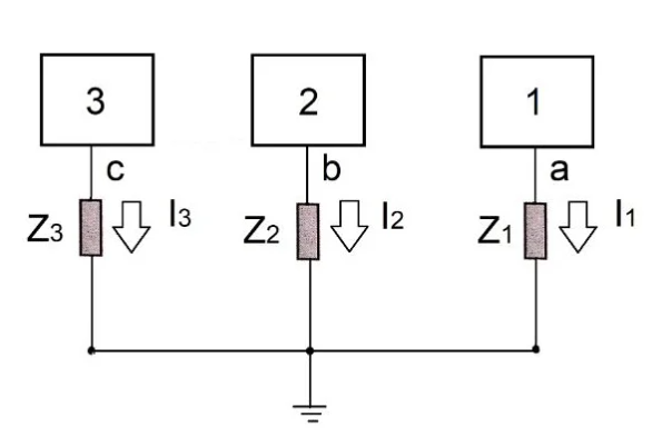
(1) Single-point grounding
This method is only suitable for applications with low interference frequencies. Ground loops can be eliminated by connecting two devices to ground using a single ground wire. Neither V1 nor V2 will form a ground loop current. The magnetic flux enclosed by the ground wire and signal lines determines the extent of external magnetic field interference. When the ground wire and signal lines are close to each other, interference is minimal.
Note that if the ground wire of device two is directly connected to the grounding point of device 1, interference will still occur. If the interference frequency is high, the effectiveness of single-point grounding is reduced. Although no obvious ground loop exists, an invisible ground loop may still be present due to distributed capacitance.
(2) Disconnect the electrical connection between the two circuits
In some cases, single-point grounding is not readily achievable. For example, for electrical safety reasons, equipment must be connected to a safety ground. In such cases, the ground loop can be eliminated by disconnecting the electrical connection between the two devices.
This can be achieved using optical couplers or isolation transformers to establish the electrical connection between the two devices. Differential signals are transmitted via light or magnetic fields. At the same time, common-mode interference generated by the ground wire is isolated: optocouplers are also commonly used to eliminate ground loops, effectively addressing the poor high-frequency isolation performance of isolation transformers. Optocouplers can achieve isolation at very high frequencies because their parasitic capacitance is only around two pF.
In environments with stricter electromagnetic interference requirements, fiber optics can be used, as they do not have the issue of parasitic capacitance and can achieve highly ideal isolation effects.
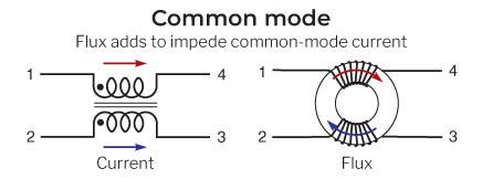
(3) Common-mode chokes
Installing common-mode chokes on cables effectively suppresses the influence of ground loop currents, as ground loop currents are common-mode currents.
Common-mode chokes reduce the impact of ground loop currents by increasing the impedance of the ground loop, thereby minimizing the influence of ground loop currents. Alternatively, part of the noise voltage is dropped across the common-mode choke, reducing its impact on the circuit. The simplest method to install common-mode chokes on interconnecting cables between two devices is to wrap the entire cable bundle around a ferrite ring.
One important point to note is that in practical applications, a larger inductance of the common-mode choke does not necessarily result in better suppression. This is because the actual common-mode choke also has distributed capacitance, which is connected in parallel with the common-mode inductance. At higher frequencies, the capacitive reactance is small, allowing interference to bypass the inductance.
(4) Balanced Circuit
A balanced circuit is one in which the impedances of two conductors and the circuits they are connected to are the same relative to Ground or another potential reference point. A differential amplifier is a typical example of a balanced circuit.
At high frequencies, circuit balance is generally poor. This is because actual circuits contain many distributed parameters, such as distributed capacitance and mutual inductance. These parameters have a significant impact on circuit impedance at higher frequencies.
Due to the uncertainty of these distributed parameters, the circuit impedance is also uncertain, making it challenging to ensure that the impedances of the two conductors are the same. Therefore, achieving complete balance in any circuit at high frequencies is exceptionally challenging.
5. Safety and EMI Considerations
5.1 Electrical Safety and Grounding
The primary methods for ensuring adequate grounding of metal enclosures to prevent electric shock include the following:
Grounding wires: Connect the metal enclosure to the Ground via a grounding wire to ensure that the potential difference between the metal enclosure and the Ground is zero. The grounding wire should be as short as possible and have sufficient conductivity to minimize ground resistance.
Grounded outlets: Ensure that electrical equipment is connected to grounded outlets, where the grounding wire can directly connect the metal housing to the grounding system.
Grounding resistance testing: Regularly test the resistance value of the grounding system to ensure it meets the required safety standards. Generally, grounding resistance should be less than 4 ohms. For critical equipment, stricter grounding resistance requirements apply.
Regular inspection and maintenance: Regularly inspect grounding wires, grounding outlets, and other grounding facilities to ensure they are in good condition. If any damage or aging is detected, replace or repair them promptly.
Prevent grounding system failure: Ensure the grounding system is not compromised by the surrounding environment, such as avoiding grounding wires that are squeezed, cut, or corroded. Additionally, ensure the grounding system maintains sufficient safety distances from other electrical systems to prevent electromagnetic interference.
l Grounding markings: Affix grounding markings on metal enclosures to alert users that the equipment is grounded, thereby enhancing user safety awareness.
Enhance personnel safety training: Strengthen employees' electrical safety knowledge training to improve their understanding of and appreciation for the grounding system, ensuring compliance with safety regulations when operating electrical equipment.
5.2 Combination of shielding layers and grounding
(1) Grounding of low-frequency cable shielding layers
In the low-frequency range, the primary purpose of shielded cables is to prevent electric field coupling from 50/60 Hz power lines. No shielding provides magnetic field protection in the low-frequency range. Shielded twisted-pair cables can be used in low-frequency applications, as the shielding layer prevents electric field coupling, while the twisted pairs prevent magnetic field coupling. After all, many low-frequency circuits contain high-impedance devices that are easily affected by electric field coupling, so low-frequency cable shielding is crucial.
In the low-frequency range, the shielding layer of multi-core cables serves as neither a signal return conductor nor a ground, and is typically grounded at only one end. If the shielding layer is grounded at more than one end, and a potential difference exists between the two ends of the cable, noise currents will flow through the shielding layer. In a single-ended grounding configuration, grounding the cable shield at the source end is preferable because it serves as the reference for the signal voltage. However, if the signal source is floating (not grounded), grounding the cable shield at the load end is preferable.
Grounding the cable shield at only one end eliminates frequency noise coupling from power lines; however, this makes the cable susceptible to RF interference, similar to a high-frequency antenna. Amplitude-modulated and frequency-modulated broadcast transmissions can induce high-frequency RF currents on the cable shielding layer.
If the cable shielding layer is connected to a grounded circuit, these RF currents will enter the equipment and may cause interference. Therefore, the correct grounding method for the shielding layer is to ground it to the equipment's shielding enclosure, not to the circuit's Ground.
The shielding layer should be connected to the shielded enclosure with the lowest possible impedance. This ensures that any RF noise currents on the shielding layer flow harmlessly along the outer surface of the enclosure and are dissipated to Ground through the enclosure's parasitic capacitance, thereby bypassing sensitive electronic equipment inside the enclosure.
If the cable shielding layer is considered an extension of the shielded enclosure, it should be connected to the enclosure's Ground with low impedance rather than to the circuit's Ground.
For coaxial cables, the shielding layer serves as the return path for the signal, so it must be grounded at both ends. Functionally, this grounding must be circuit ground.
However, for noise considerations, the shielding should first terminate at the enclosure. This can be achieved by terminating the cable shielding layer at the enclosure and then connecting the circuit ground to the same point on the enclosure.
Single-ended shield grounding is adequate at low frequencies (audio and below) because it prevents power frequency currents from flowing through the shield and introducing potential noise into the signal circuit. Single-point grounding also eliminates shield ground loops and potential magnetic field coupling.
However, as frequency increases, single-point grounding becomes increasingly ineffective. When the cable length approaches one-quarter of the wavelength, a shielded cable with one end grounded becomes a highly effective antenna. In such cases, it is typically necessary to ground both ends of the shielding layer.
(2) High-frequency cable shield grounding
When the frequency exceeds 100 kHz or the cable length exceeds one-twentieth of the wavelength, the shield must be grounded at both ends (or at multiple points). This applies to both multi-conductor cables and coaxial cables. Another issue caused by high frequencies is stray capacitance, which forms ground loops, making it difficult or impossible to isolate the non-terminated end of the shield from Ground.
Therefore, in high-frequency and digital circuits, it is common practice to ground both ends of the cable shielding layer. At frequencies above 1 MHz, the skin effect reduces the common impedance coupling between the signal and noise currents flowing through the shielding layer. The skin effect causes noise currents to flow along the outer surface of the shielding layer, while signal currents flow along the inner surface. Multi-point grounding also provides magnetic field shielding at frequencies above the cutoff frequency of the shielding layer.
(3) Mixed cable shield grounding
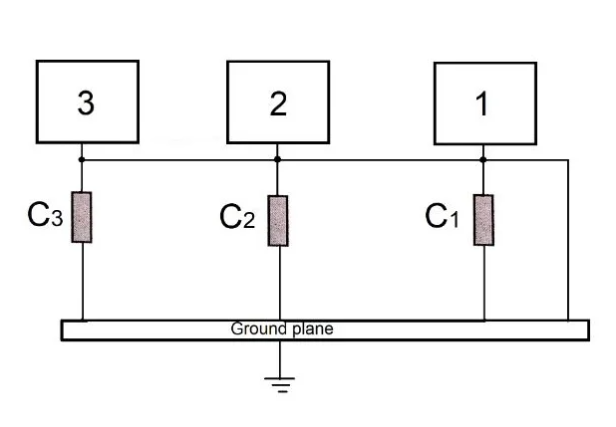
Single-point grounding is sufficient at audio frequencies and below, while multi-point grounding is suitable for high frequencies. However, what should be done when the signal contains both high- and low-frequency components? In this case, the parasitic capacitance can be replaced with an actual capacitor (e.g., 47nF) to form a combined or mixed grounding configuration. At low frequencies, single-point grounding exists because the capacitance has high impedance. At high frequencies, the capacitance becomes low impedance, converting the circuit into a two-point grounding configuration.
However, effectively implementing hybrid cable shield grounding may be challenging in practice, as any inductance in series with the capacitance reduces its effectiveness. Ideally, the capacitance should be integrated into the connector.
(4) Grounding of double-shielded cables
There are two scenarios for using double-shielded cables: first, to enhance high-frequency shielding performance, where the two shielding layers can be in contact with each other; second, when both high-frequency and low-frequency signals coexist within the same cable, in which case the two shielding layers must be electrically isolated (commonly referred to as a three-coaxial cable).
When the two shielding layers are insulated from each other, different termination methods can be selected for each shielding layer. The outer shielding layer can be terminated at both ends to provide adequate shielding against high-frequency and magnetic fields.
Additionally, the outer shielding layer prevents radiation caused by high-frequency common-mode currents on the cable. The inner shielding layer can be terminated at only one end to avoid ground loop coupling when both ends are grounded.
In practice, the inner shield is terminated at low frequencies, while the outer shield is terminated at high frequencies. The outer shield should be connected to the chassis, and the inner shield should be connected to the housing or the circuit ground. Both methods provide good performance.
When using dual shielding layers, another termination method involves terminating both shielding layers at one end but on opposite ends. In this case, there are no low-frequency ground loops, and the capacitance between the shielding layers closes the high-frequency path. This approach is practical when the cable is very long.
5.3 Avoiding Ground Bounce and Ground Noise
At low frequencies, ground noise is primarily caused by the "resistance" of the conductors forming the ground line, resulting in potential fluctuations as current flows through the ground line. At high frequencies, ground noise is primarily caused by the 'inductance' of the conductors forming the ground line. When current rapidly changes and flows through this "inductance," it induces stronger voltage disturbances at the two ends of the "inductance," which is metaphorically referred to as "ground bounce."
Ground bounce generally affects ICs. This is because the "circuit ground" inside the chip and the chip's "ground pin" are connected by a skinny gold wire, resulting in significant inductance. This can cause strong voltage fluctuations between the Ground of the internal circuit and the actual PCB ground—this is known as the ground bounce phenomenon.
What methods can be used to mitigate ground bounce?
(1) Consider adding a soft-start circuit in the circuit to gradually increase the power supply voltage, reduce initial current surges, and avoid large current transients (Inrush Current) when the device powers on, thereby reducing ground bounce noise.
(2) During PCB design, ensure that the ground network on two-layer boards is sufficiently broad and extensively connected. For multi-layer boards, maintain an intact ground plane, minimize loop inductance, reduce ground plane segmentation, and prevent sudden changes in return paths.
(3) IC ground pins should be routed as short and wide as possible or connected to the complete ground plane via multiple vias to reduce parasitic inductance. For high-speed ICs, local ground copper can be placed beneath the chip and connected to the central ground plane via resistance paths.
(4) Ground loops in power circuits must be managed appropriately. This can be achieved by reducing the switching speed of switching devices (e.g., adjusting the drive resistance of MOSFETs) or using soft-switching techniques (e.g., ZVS/ZCS) to minimize transient current surges, thereby reducing current changes and avoiding ground bounce.
(5) Minimize the number of loads operating simultaneously during startup and avoid switching integrated circuit switches at the same time to reduce peak transient currents, thereby mitigating voltage fluctuations caused by parasitic inductance.
6. Application of GND in actual operation and measurement
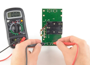
6.1 How to find GND with a multimeter
a. Connect the black probe of the multimeter to the COM port and set it to the buzzer mode.
b. Touch the black probe to the antenna and the red probe to any interface. If a buzzer sound is heard at any interface, that interface is GND.
6.2 The Importance of Grounding Oscilloscope Probes
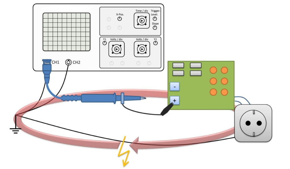
(1) Ensure measurement accuracy
First, grounding is a critical factor in ensuring measurement accuracy. If the oscilloscope probe is not grounded, it may introduce ground loop interference, causing unnecessary noise to be mixed into the measurement signal. This noise distorts the original signal, resulting in distorted measurement results.
By properly grounding the oscilloscope, these interferences can be effectively eliminated, ensuring the purity and accuracy of the measurement signal.
In scientific research and industrial production, accurate measurement data is the basis for decision-making and improvement, and even the slightest error can lead to significant deviations.
(2) Safety
Second, grounding is critical to the safety of operators. When measuring high-voltage circuits, ungrounded probes can cause static electricity to accumulate, increasing the risk of electric shock. Proper grounding safely dissipates this static electricity, protecting operators from electric shock.
Additionally, grounding prevents equipment damage caused by static discharge, extending the equipment's service life. In laboratory and production environments, safety is always the top priority, and proper grounding measures are a critical component of ensuring safety.
(3) Minimizing Interference
Furthermore, grounding helps reduce electromagnetic interference, ensuring signal purity. In complex electromagnetic environments, ungrounded probes are susceptible to interference from external electromagnetic fields, leading to distorted or unclear waveforms.
Grounding effectively shields these interferences, making measurement signals more stable and reliable. This is particularly important for applications that require high-precision measurements, such as medical equipment, aerospace, and precision instrument manufacturing.
(4) Preventing common-mode interference
In differential measurements, grounding effectively prevents common-mode interference. Common-mode interference refers to the same interference signal appearing simultaneously at two measurement points. If not grounded, these interference signals will superimpose on the differential signal, causing measurement errors.
Proper grounding eliminates common-mode interference, making differential signal measurements more accurate. This is of great significance in applications requiring high-precision differential measurements, such as communication systems and precision control systems.
(5) Compliance with standards and specifications
Ultimately, proper grounding is necessary to meet relevant safety standards and operational requirements. In many industries and applications, such as electronics manufacturing, power systems, and research laboratories, there are explicit standards and specifications requiring equipment to be grounded.
Compliance with these standards and specifications not only ensures measurement accuracy and safety but also avoids legal liability and losses resulting from non-compliance.
6.3 Grounding in Single-Power and Dual-Power Circuits
There are significant differences between grounding in single-power and dual-power circuits, primarily in terms of power supply methods, signal processing, grounding design, and application scenarios.
(1) Power Supply Methods and Signal Processing
A single power supply provides only a single positive and negative voltage level (e.g., +30V/0V). Signal processing requires a bias voltage above the positive power rail and cannot directly process negative voltage signals. Op-amp outputs cannot truly reach ground potential, resulting in a minimum output voltage limit, which requires additional bias circuits.
Dual Power Supply Provides positive and negative voltage levels (e.g., ±15V), allowing signals to cross the zero potential naturally. Op-amp outputs can reach ground potential, offering a wider input range. The static point is at zero potential, simplifying DC bias design and providing more symmetrical dynamic range.
(2) Grounding design
In a single-supply configuration, the signal ground and power ground are combined, and all components are connected to the same ground plane. Coupling capacitors are required to isolate the signal from the power supply. The ground loop is complex, prone to noise interference, and single-point grounding limits high-frequency signal processing.
In a dual-power supply configuration, the signal ground and power ground are separated (e.g., the "ground" in a dual-power supply), reducing ground loops and minimizing noise coupling. Input/output coupling capacitors can be directly connected without considering the bias point, simplifying the design.
(3) Application scenarios and advantages/disadvantages
Single-power supply systems are cost-effective and easy to install but have limited signal processing capabilities, making them suitable for applications with low negative voltage requirements. Dual-power supply systems offer superior signal processing capabilities and are ideal for analog circuits and differential signals, but they are more complex in terms of cost and wiring.
6.4 Example demonstration: LED not lighting up due to GND issues
7 common GND issues and solutions:
| Fault symptoms | Root cause | Solutions | Verification method |
|
LED Dead |
GND open |
Resolder/replace wiring, focus on connectors |
Continuity Range Segmented Testing |
|
LED dimness |
Long Trace Resistance |
Upgrade to ≥0.5mm² wire and widen PCB ground traces |
LED cathode voltage check (>0.3V = fault) |
|
Power-on transient illumination |
Cold Solder Joint (Ground) |
Re-solder GND pad and remove oxidation |
LED Temporary Recovery During Soldering |
|
Partial LED Failure |
Daisy Chain Ground → Remote Voltage Drop Accumulation |
StarGrounding (All LED cathodes directly to power negative) |
LED Cathode Voltage Differential (Near/Far) |
|
Touch-to-GND LED Activation |
Floating GND |
PS_NEG-to-GND continuity check |
Measure resistance between GND net and power negative terminal |
|
Switching Flicker |
Ground bounce |
Place 100μF + 0.1μF capacitors in parallel near the LED side of GND |
Oscilloscope observation of GND noise (>50mVpp abnormal) |
|
LED anomaly on PCB |
GND via crack and thermal pad over-cooling |
PCB Rework: Solder Mask Scraping & GND Via Optimization |
Microscopic Via Inspection & Thermal Imaging Analysis |
7. Frequently Asked Questions
7.1 Can GND be floating?
Whether GND (ground) is floating depends on the specific application scenario.
In most cases, GND serves as the reference potential point for a circuit and must be connected to earth or the negative terminal of the power supply to form a stable zero potential reference, such as protective grounding or signal grounding, and is therefore non-floating. However, in specific circuit designs (such as floating ground technology), GND can be disconnected from the earth and only coupled with other circuits through capacitors or other isolation components to suppress interference or achieve high-voltage isolation, making it floating.
In summary, GND can be either fixed (connected to the earth or the power supply's negative terminal) or floating (not directly connected to the earth), depending on the circuit's requirements.
7.2 Must all modules be grounded together?
In circuits composed of multiple PCBs, grounding is typically required to maintain signal integrity and system stability.
Grounding reduces ground potential differences and avoids interference caused by ground loop currents. If the system is susceptible to interference and the PCB modules can be physically isolated and use independent power supplies, grounding may not be necessary.
However, in such cases, additional isolation measures, such as optocouplers or transformers, must be implemented to prevent signal interference.
Grounding is typically implemented using single-point grounding or multi-point grounding to ensure consistent ground potential across all PCBs. Low-impedance grounding paths should be used to minimize ground potential differences and ground loop currents.
7.3 Are GND and 0V the same thing?
Ideally, GND is 0V, which is the reference point for voltage measurement.
However, in real circuits, due to the impedance of wires/PCB traces, a voltage drop (ground bounce effect) occurs when current flows through GND, causing the potential of the physical GND point to not be exactly 0V, especially in high-current or high-frequency systems.
0V is a theoretical reference value, while GND is the physical path for current return. When designing high-precision circuits, techniques such as star grounding and ground plane segmentation should be employed to minimize the deviation between GND and 0V. Additionally, measurements should always be verified with the power supply's negative terminal as the reference point.
Recommended Reading:
Zero-Ohm Resistor