The Arrow, the Bubble, and the Gate Decoding the PMOS Transistor Symbol
In the intricate tapestry of electronic circuit schematics, symbols serve as the universal language, condensing complex physical devices and profound electrical behaviors into concise, recognizable glyphs. Among these, the PMOS Transistor Symbol stands as a crucial yet sometimes understated element. Representing a fundamental building block of modern integrated circuits, particularly within Complementary MOS (CMOS) technology, its visual representation – a simple combination of lines, angles, and a distinctive bubble – encodes a wealth of information about its structure, function, and electrical characteristics. Understanding the PMOS symbol is essential for navigating circuit diagrams, designing robust electronics, and appreciating the elegant abstraction that underpins digital and analog design. This article delves into the anatomy, evolution, standardization, and profound meaning embedded within this seemingly simple icon.
The Foundational Dichotomy: NMOS vs. PMOS
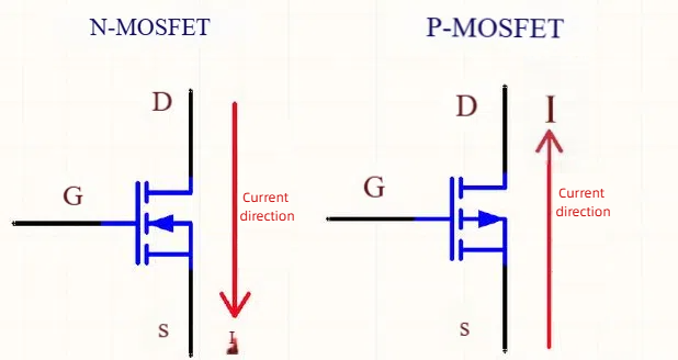
Before dissecting the PMOS symbol, its significance is best understood within the context of its counterpart, the NMOS (N-channel MOS) transistor. MOS transistors are voltage-controlled switches or amplifiers, their operation governed by an electric field generated by a negative voltage applied to the gate terminal. The core difference lies in the type of charge carrier they primarily use:
1.NMOS: Conducts using electrons (negative charge carriers) as the majority carrier in its channel when turned on. Requires a positive gate-to-source voltage (V_GS) exceeding a threshold voltage (V_th) to conduct.
2.PMOS: Conducts using flow of holes (effectively positive charge carriers) as the majority carrier in its channel when turned on. Requires a negative gate-to-source voltage (V_GS) exceeding a threshold voltage (V_th – typically negative) to conduct. In digital circuits, this often means the gate voltage needs to be lower than the source voltage by a sufficient amount.
This fundamental difference in carrier type and positive voltage polarity requirement is the cornerstone reflected in their distinct schematic symbols.
Deconstructing the Symbol: Anatomy of the PMOS Glyph
The standard PMOS transistor symbol shares a common skeletal structure with the NMOS symbol but incorporates key differentiating elements:
1.The Channel Line: A central horizontal line representing the conductive path (channel) between the source and drain terminals. This is the core structural element shared with NMOS.
2.The Gate Terminal: A vertical line perpendicular to the channel line, representing the gate electrode, separated by the thin oxide layer (implied by the gap). This gate controls the conductivity of the channel.
3.The Source and Drain Terminals: Lines extending outward from the ends of the channel line. By convention in many schematics:
● The terminal connected to the higher voltage potential (often the positive supply rail, VDD, in digital circuits) is the Source for a PMOS transistor.
● The terminal connected to the lower voltage potential (often ground or the output node) is the Drain for a PMOS transistor.
● Crucially, the physical source and drain are often interchangeable in structure, but their functional designation in the symbol depends on the circuit context and voltage level.
4.The Substrate/Body Terminal: A line connected to the channel line, usually angled at 45 degrees or perpendicular, pointing inwards towards the channel. This represents the bulk silicon substrate (for discrete devices) or the well (in integrated circuits) in which the field-effect transistor is fabricated.
5.The Defining Bubble (or Arrow): This is the most critical distinguishing feature:
● The "Bubble" Convention (IEEE Std 315 / Common Practice): A small circle is placed on the gate terminal where it meets the gate line. This bubble signifies that the transistor is active-low or inverting in its control logic. For a PMOS, this directly corresponds to the requirement of a low (or negative) gate voltage relative to the source to turn the transistor ON (conducting). This is the predominant symbol in North America and many global schematics.
● The Arrow Convention (Less Common, Often IEC-influenced): An arrow is placed on the substrate/body terminal, pointing towards the channel. For a PMOS transistor, this arrow points inwards. This signifies the direction of hole current flow when the electronic device is conducting – holes flowing from the source to the drain. The NMOS arrow points outwards (electron flow from source to drain). While standardized in IEC 60617, this form is less common in many contemporary digital IC schematics compared to the bubble-on-gate.
Table 1: Core Elements of the PMOS Transistor Symbol
| Element | Visual Description | Meaning/Function |
|---|---|---|
|
Channel Line |
Horizontal line |
Represents the conductive path between Source and Drain. |
|
Gate Terminal |
Vertical line perpendicular to channel (with gap) |
Control electrode. Voltage here determines channel conductivity. |
|
Source Terminal |
Line at one end of channel |
Terminal typically at higher voltage (
). Point where carriers (holes) enter the channel when ON. |
|
Drain Terminal |
Line at the other end of channel |
Terminal typically at lower voltage. Point where carriers (holes) exit the channel when ON. |
|
Substrate/Body |
Line angled inwards (45° or perp.) touching channel |
Represents the bulk silicon or well connection. Usually tied to the highest potential (
) for PMOS in ICs. |
|
Bubble (Gate) |
Small circle on Gate line |
Standard IEEE/Common: Indicates active-low control (ON when gate is LOW relative to source). |
|
Arrow (Body) |
Arrowhead on Substrate/Body line pointing INWARDS |
IEC Standard/Less Common: Indicates hole current flow direction (inwards) and identifies PMOS type. |
Evolution and Standardization: From Physical to Abstract
Like many schematic symbols, the PMOS representation evolved from attempts to pictorially represent the physical device performance:
1.Early Depictions: Early schematics might have shown more literal representations, perhaps hinting at the metal gate, oxide layer, and p-type depletion regions for the source, drain, and channel within an n-type substrate or well. These were cumbersome for digital logic circuits.
2.The Emergence of the Standard: The need for clarity, speed of drafting, and universality drove abstraction. The core structure (source, gate, drain, substrate) was retained, while the physical details were stripped away. The key differentiator became the indicator of channel type and control logic.
3.Standardization Bodies:
● IEEE Std 315: This is the dominant standard in North America and widely used globally. It firmly establishes the PMOS symbol with the bubble on the gate terminal and the substrate/body connection. The substrate arrow is not part of the primary IEEE symbol for MOS transistors; the bubble is the key identifier.
● IEC 60617 (International Standard): IEC standards often use the arrow on the substrate/body terminal pointing inwards to denote a PMOS transistor. The gate bubble is typically not used in this convention. Some European or IEC-compliant schematics favor this style.
● ANSI Y32.2: Often aligns with IEEE standards in the US.
The "Bubble Controversy" and Practical Usage
The coexistence of the "bubble-on-gate" (IEEE) and "arrow-on-body" (IEC) conventions can cause confusion, especially for those encountering different schematic styles. However, practical usage in modern electronics, particularly digital IC design, heavily favors the bubble-on-gate symbol for PMOS, often omitting the substrate/body connection entirely in high-level schematics. Why?
1.Functional Clarity (Digital Logic): In digital CMOS circuits, PMOS and NMOS transistors work together as complementary switches. The bubble on the PMOS gate provides immediate visual feedback on its logic behavior: it turns ON when its input (gate voltage) is LOW (0). The NMOS, lacking a bubble, turns ON when its input is HIGH (1). This directly mirrors the logic gates they form (e.g., a PMOS pull-up network activated by LOW inputs and an NMOS pull-down network activated by HIGH inputs in an inverter or NAND gate). The bubble is a direct indicator of the inversion required for PMOS control.
2.Substrate Connection Implied: In integrated circuits, the substrate/body of all PMOS transistors within an n-well is almost invariably connected to the highest positive supply voltage (VDD). Because this connection is nearly universal and constant within a block, it is frequently omitted from high-level schematic symbols to reduce clutter. The presence of the PMOS bubble is sufficient identification.
3.Emphasis on Control Logic: The bubble prioritizes conveying the voltage level needed for conduction, which is paramount for understanding circuit design, over the physical carrier type (implied by the PMOS type).
Variations and Enhanced Symbols
While the basic bubble-on-gate PMOS is most common, variations exist to convey additional information:
1.Explicit Substrate/Body: Often included in analog circuit schematics, discrete device schematics, or when body biasing is a critical design consideration. The connection line points inwards.
2.Dual-Gate PMOS: Rare, but used in some RF or specialized analog circuits. Represented by two parallel gate lines extending from the main gate terminal. The bubble is still placed on the gate input line.
3.Depletion-Mode PMOS: Extremely rare compared to depletion-mode NMOS. If depicted, might use a solid channel line instead of the broken/dashed line sometimes used for depletion NMOS. The gate bubble remains. (Note: The broken/dashed line convention for depletion mode is not universally standardized and often requires a note).
4.4-Terminal Symbol (Explicit Body): Used when the body terminal's connection is not to VDD and needs explicit representation, crucial for analyzing body effect (where body-source voltage V_BS modulates the threshold voltage V_th).
The Profound Meaning Encoded: Physics and Polarity
The PMOS symbol, particularly the bubble or the inward-pointing arrow, is not merely an arbitrary mark; it encapsulates fundamental semiconductor physics:
1.Majority Carrier: The bubble/arrow signifies the use of holes as the primary charge carrier. Holes are vacancies in the crystal lattice that behave like positive charges.
2.Voltage Polarity Requirement: The bubble explicitly indicates the negative V_GS requirement for conduction. For the PMOS to turn ON and conduct significant current (I_DS), the gate voltage (V_G) must be sufficiently lower than the source voltage (V_S). V_GS < V_th (where V_th is negative). This is why PMOS is the natural choice to connect between VDD (high) and an output: it conducts when its gate is pulled LOW (towards ground), pulling the output HIGH.
3.Current Flow Direction: While the symbol doesn't explicitly show current direction like a diode, the functional designation (Source = higher potential, Drain = lower potential) combined with hole conduction implies conventional current flows from Source to Drain when the PMOS is ON. (Conventional current direction is opposite to electron flow but aligns with hole flow direction).
4.Complementary Nature: The symbol only gains its full power in conjunction with the NMOS symbol. The absence of a bubble on NMOS and its presence on PMOS visually reinforces their complementary switching behavior in CMOS logic, the bedrock of modern digital electronics. This complementary pairing minimizes static power consumption.
The Symbol in Action: Reading PMOS in Circuits
Understanding the symbol allows engineers to instantly grasp the key role of a PMOS transistor in a schematic:
1.CMOS Inverter: The archetypal circuit design. A PMOS (with gate bubble) connects VDD to the output. An NMOS (no bubble) connects the output to GND. When input (connected to both gates) is HIGH, NMOS ON (pulls output LOW), PMOS OFF. When input LOW, PMOS ON (pulls output HIGH), NMOS OFF. The bubble visually explains why the PMOS acts when the input is LOW.
2.CMOS NAND Gate: Two PMOS transistors (both with bubbles) connected in parallel between VDD and output. Two NMOS transistors (no bubbles) connected in series between output and GND. The output is HIGH (via PMOS) only if both inputs are LOW (activating both PMOS). If either input is HIGH, the corresponding PMOS turns OFF, and if both inputs HIGH, the series NMOS turn ON, pulling output LOW. The bubbles on the PMOS gates immediately show they require LOW inputs to conduct.
3.Analog Switches & Transmission Gates: A PMOS can be used alone as a switch controlled by a negative gate voltage relative to source. More commonly, a PMOS and NMOS are connected in parallel (source-source, drain-drain) to form a transmission gate, passing signals bidirectionally when their complementary gate controls (one inverted signal) are applied. The symbols clearly show the complementary control.
4.Power Management: PMOS transistors are often used as high-side switches (between VDD and load) because their source is naturally at VDD. The symbol shows this connection directly. Driving the gate LOW turns on the load.
5.Amplifiers (Less Common): While NMOS dominates single-ended amplifiers due to better electron mobility, PMOS devices are used in differential pairs (complementary stages) or as current sources/loads. The symbol identifies the digital device type and polarity requirements for biasing.
Table 2: PMOS Symbol Interpretation in Key Circuit Roles
| Circuit Role | Typical Symbol Context | Symbol Tells You |
|---|---|---|
|
CMOS Pull-Up (Inverter/NAND/NOR) |
Connected between
and output node. Gate connected to input signal(s). Bubble present. |
"This device will conduct (pull output HIGH) when its gate signal(s) are LOW." |
|
High-Side Switch |
Connected between positive supply (
/
) and load. Source at supply. Gate control signal. Bubble present. |
"This device will turn ON (connect supply to load) when the gate control signal is LOW (relative to source/supply)." |
|
Transmission Gate (Part) |
Source/Drain connected to one side of signal path. Gate connected to control signal (often inverted). Bubble present. |
"This device will pass the signal (bidirectionally) when its gate control is LOW." (Requires complementary NMOS with HIGH control). |
|
Current Source/Load (Analog) |
Source at
, Gate biased with fixed voltage, Drain feeding circuit node. Bubble present. |
"This is a PMOS device acting as a current source/sink. Gate bias voltage must be sufficiently below |
|
Differential Pair (Part) |
Source(s) tied together to tail current source, Gates = differential inputs, Drains = outputs. Bubble present. |
"These are PMOS input transistors. Increasing the gate voltage (making it less negative relative to source) decreases their current." |
Beyond the Lines: A Symbol of Complementarity and Control
The PMOS transistor symbol is far more than a drawing convention. It is a vital piece of the visual vocabulary that enables the design and understanding of the complex electronic systems that define our world. Its seemingly simple addition of a bubble or an arrow encodes the physics of hole conduction, the requirement for negative gate control, and its crucial role as the complement to the NMOS transistor.
The elegance of the PMOS symbol lies in its ability to abstract away the intricate details of semiconductor fabrication and electric fields within silicon dioxide, focusing the designer's mind on the fundamental electrical behavior: a voltage-controlled switch that conducts when its gate is low. It embodies the principle of complementarity that makes CMOS technology so powerful and efficient.
In the dense schematics of microprocessors, memory chips, power converters, and sensor interfaces, the PMOS symbol, with its distinctive bubble or inward-pointing arrow, stands as a silent testament to the ingenuity of semiconductor physics and the power of visual abstraction. It is a glyph that bridges the gap between the microscopic world of doped silicon and the macroscopic world of electronic function, enabling the creation of the technology that shapes our modern existence. Understanding its nuances is fundamental for anyone navigating the world of electronic design.