MOSFET vs. BJT: Key Differences and How to Choose
A MOSFET is a type of transistor. So, comparing a MOSFET with a transistor usually means comparing it with a BJT (Bipolar Junction Transistor). This article uses "BJT" for this comparison.
Both devices can switch a load or amplify a signal, and a datasheet rarely settles the choice on its own. The better part depends on load current, available drive voltage, switching frequency, power budget, and what the part must cost and how easily it can be bought in volume.
This guide is written for engineers, makers, and buyers selecting a part for a real circuit. It works from operating conditions rather than theory: a worked switching example, amplifier use, operating limits, datasheet reading, and the path from shortlist to purchase. The numbers come from the datasheets of real, widely stocked parts, so each claim can be checked. For definitions and operating principles, see What Is a MOSFET and How Does a MOSFET Transistor Work.
Quick Answer: Which Device for Which Job
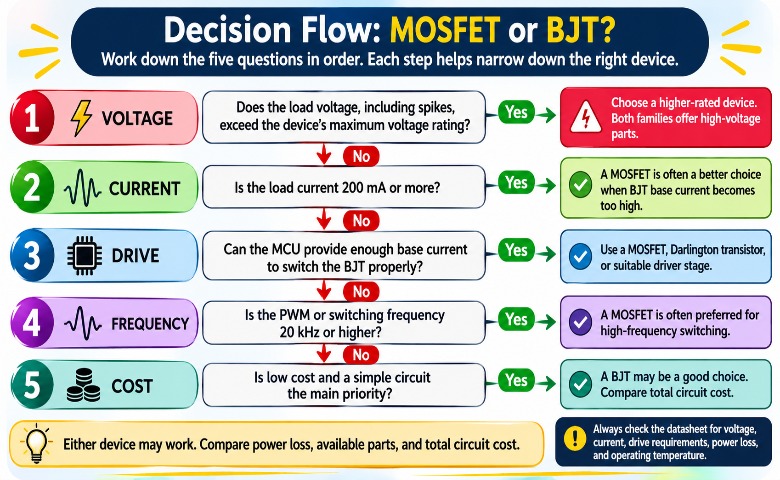
You can choose between a MOSFET and a BJT by asking five simple questions:
- What voltage does the load need?
- How much current does the load use?
- What voltage and current can the control circuit provide?
- How fast does the device need to switch?
- What is the budget, and how many units are needed?
| Application | Start with | Main reason | Details in |
|---|---|---|---|
| Indicator LED / small relay driver | BJT | Low cost and simple switching for small loads | Switching and MCU Drive |
| LED strip PWM dimming | Logic-level MOSFET | Low power loss and efficient PWM dimming at higher currents | Switching and MCU Drive; Operating Limits |
| Small DC motor / fan | MOSFET | Lower voltage drop and less heat | Switching and MCU Drive |
| Solenoid or valve | MOSFET | Handles higher currents with low power loss and flyback protection | Switching and MCU Drive |
| Audio preamp / sensor amplifier | BJT, or MOSFET for high-impedance sources | BJT for suitable low-noise gain; MOSFET for high input impedance | Amplifier Circuits |
| Battery-powered load switch | MOSFET | Very low gate leakage and low power loss when properly selected | Operating Limits |
| Automotive low-side driver | MOSFET, automotive-grade | Automotive qualification, voltage protection, and thermal reliability | Datasheets; Operating Limits |
Treat this table as a guide, not a strict rule. A small indicator LED drawing well under 20 mA can often connect directly to an MCU pin through a current-limiting resistor, without a MOSFET or BJT. Always check the MCU's pin current limits.
A BJT relay driver may need too much base current when the coil current is high. For example, with a forced beta of 10, a 100 mA relay coil needs about 10 mA of base current.
The switching recommendations in this table assume low-side N-channel MOSFETs or NPN BJTs. High-side circuits may need different devices and designs. For high-side switching and P-channel parts, see N-Channel vs. P-Channel MOSFET.
The examples below use the PN2222A, 2N3904, TIP120, 2N7002, IRLML6344, and AO3400A. Values are taken from the datasheets, and typical values are labeled. Maximum ratings are not recommended operating values. Always check the datasheet for the exact part and manufacturer you buy.
Switching and MCU Drive: One Load, Two Circuits
The test load
Each example in this section uses the same load: 12 V at 500 mA (24 Ω), switched on the low side. The control signal comes from either a 5 V Arduino-class pin or a 3.3 V ESP32/STM32-class pin.
The two devices are an onsemi PN2222A BJT (TO-92) and an Infineon IRLML6344TRPbF MOSFET (SOT-23). Values below are taken from the manufacturers' datasheets. Maximum, minimum, and typical values are identified where relevant.
An ATmega328P pin (Arduino Uno) has an absolute maximum current rating of 40 mA. However, 20 mA is the commonly used design value at 5 V. Many 3.3 V MCUs have different GPIO limits, so always check the datasheet.
BJT circuit: base current is the cost of switching
The PN2222A datasheet guarantees VCE(sat) ≤ 1.0 V at IC = 500 mA, but only with IB = 50 mA, a forced beta of 10. The base resistor follows from RB = (VDRIVE − VBE(sat)) / IB. VBE(sat) is specified up to 2.0 V at this point, so a 5 V pin needs about 60 Ω and a 3.3 V pin about 26 Ω. At 3.3 V only 1.3 V remains across the resistor, so the base current becomes sensitive to VBE spread.
Either way, the pin would need to source 50 mA, which is above its 40 mA absolute maximum rating. The ATmega328P also does not guarantee its output voltage at this current. At a 5 V supply, it guarantees an output-high voltage of at least 4.2 V at a 20 mA load. This means the pin may not maintain the required voltage when asked to supply 50 mA.
The PN2222A has a minimum DC current gain of 40 at a collector current of 500 mA and a collector-emitter voltage of 10 V. This gives a calculated base current of 12.5 mA in that test condition. However, this does not guarantee saturation. For the datasheet's guaranteed saturation voltage of 1.0 V at 500 mA, the required base current is 50 mA.
Common solutions include a Darlington transistor, a separate driver stage that supplies the required base current, or a different switching device.
MOSFET circuit: voltage, not current
The IRLML6344 gate draws only leakage at DC (IGSS ≤ 100 nA). The datasheet guarantees RDS(on) ≤ 37 mΩ at VGS = 2.5 V and ≤ 29 mΩ at 4.5 V, so a 3.3 V pin is covered. A MOSFET listed only at 10 V carries no such guarantee on logic-level drive. The absolute maximum VGS is ±12 V, so the gate must never be tied to the 12 V load rail.
Gate resistors, pull-downs, and gate-charge timing are covered in MOSFET Switch: How to Use a MOSFET as a Switch. For pins too weak to charge the gate, see Gate Drivers: How They Work, Types, and Selection Guide.
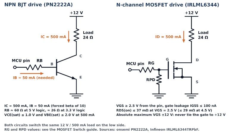
| 5 V logic vs 3.3 V logic | 5 V logic | 3.3 V logic |
|---|---|---|
| BJT base resistor for IB = 50 mA (VBE(sat) = 2.0 V) | 60 Ω | 26 Ω |
| Pin current the BJT needs | 50 mA | 50 mA |
| MOSFET RDS(on) guarantee (IRLML6344) | ≤ 29 mΩ at 4.5 V | ≤ 37 mΩ at 2.5 V |
| MOSFET gate voltage | Well above 2.5 V, below ±12 V | About 0.8 V above the 2.5 V point |
Moving from 5 V to 3.3 V does not solve the BJT's base-current problem. It still needs 50 mA to meet the PN2222A's specified saturation condition. This is too much for a typical MCU GPIO pin.
A 3.3 V signal also provides less gate drive than a 5 V signal. However, the IRLML6344 has a guaranteed RDS(on) rating at 2.5 V, which is below the 3.3 V logic level. This makes it a suitable choice for 3.3 V control, provided the actual gate voltage reaches the required level.
The 0.8 V difference between 3.3 V and the 2.5 V test point is useful to note, but it should not be treated as a guaranteed safety margin. Always check the MCU's actual output voltage and the MOSFET's datasheet specifications.
| Conduction loss and heat | PN2222A (BJT) | IRLML6344 (MOSFET) |
|---|---|---|
| Control requirement | IB = 50 mA | VGS ≥ 2.5 V, very low DC gate current |
| On-state drop at 500 mA | VCE(sat) ≤ 1.0 V | 0.5 A × 37 mΩ = 18.5 mV |
| Estimated device dissipation | 0.50 W collector + 0.10 W base = 0.60 W | 0.5² × 0.037 = 9.25 mW |
The PN2222A is rated for 625 mW of total device dissipation at 25°C ambient. Its junction-to-ambient thermal resistance is 200°C/W, and its maximum junction temperature is 150°C. A theoretical 0.60 W loss would produce a temperature rise of about 120°C. At a 30°C ambient temperature, this would reach the 150°C junction limit, leaving no thermal margin.
However, the PN2222A's specified saturation values at 500 mA are measured using short pulses, not continuous operation. Therefore, the 0.60 W figure is an estimate based on those datasheet limits, not a guarantee of continuous performance.
At 25°C, the IRLML6344's estimated conduction loss is only 9.25 mW using its maximum RDS(on) of 37 mΩ. Its on-resistance increases with temperature, so check the datasheet's temperature curve when estimating hot operating conditions. Even if the resistance doubled, conduction loss would remain below 20 mW.
A lighter load where the BJT works
Reduce the load to 12 V at 150 mA, and the comparison changes. The PN2222A datasheet specifies a maximum VCE(sat) of 0.3 V at a collector current of 150 mA and a base current of 15 mA. At this test condition, VBE(sat) is specified up to 1.2 V.
Using the maximum VBE(sat), the calculated base resistor is about 253 Ω for a 5 V signal and 140 Ω for a 3.3 V signal. The required base current of 15 mA is within the commonly used 20 mA design value for an ATmega328P pin. However, always check the GPIO limits of your specific MCU.
| Comparison | PN2222A (BJT) | IRLML6344 (MOSFET) |
|---|---|---|
| Control requirement | IB = 15 mA | VGS ≥ 2.5 V |
| On-state drop at 150 mA | VCE(sat) ≤ 0.3 V | About 5.6 mV |
| Estimated conduction loss | 45 mW collector + 18 mW base = 63 mW | About 0.8 mW |
Both devices can work for this load. The BJT's estimated 63 mW power loss would produce a temperature rise of about 13 °C at 200 °C/W, under the stated calculation. The MOSFET still wastes much less power, but the BJT can be a reasonable choice when cost, available parts, and the MCU pin's current limit are considered. Remember that the PN2222A's saturation figures are based on short-pulse testing, not guaranteed continuous operation.
The low-current crossover
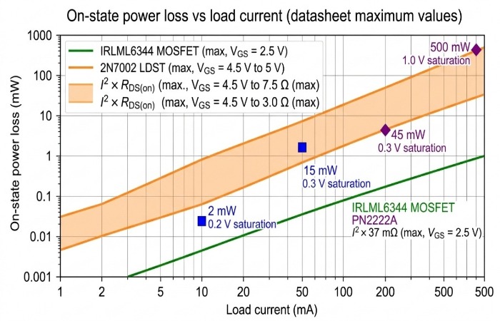
A common claim says that a BJT is better than a MOSFET at low current. However, the datasheets show that this is not always true. The result depends on which MOSFET is being compared.
A BJT has a relatively fixed voltage drop when switched on. For example, the 2N3904 specifies a maximum VCE(sat) of 0.2 V at 10 mA and 0.3 V at 50 mA, with a base current equal to one-tenth of the collector current. A MOSFET's voltage drop depends on its on-resistance and load current. As the load current decreases, its voltage drop also decreases.
| Load current | 2N3904 VCE(sat) max | 2N7002 at 7.5 Ω | 2N7002 at 3.0 Ω | IRLML6344 at 37 mΩ |
|---|---|---|---|---|
| 10 mA | 0.2 V | 75 mV | 30 mV | 0.4 mV |
| 50 mA | 0.3 V | 375 mV | 150 mV | 1.9 mV |
| 100 mA | Not specified | 750 mV | 300 mV | 3.7 mV |
| 200 mA | Not specified | 1.5 V | 0.60 V | 7.4 mV |
The 2N7002 values in the table show two different manufacturer specifications. Some datasheets specify a maximum RDS(on) of 7.5 Ω at a 5 V gate drive, while others specify 3.0 Ω at 4.5 V. With the 7.5 Ω version, the MOSFET's voltage drop reaches the 2N3904's specified range at around 27–40 mA. With the 3.0 Ω version, this happens at around 67–100 mA.
These crossover values are estimates, not universal limits. The 2N3904's guaranteed saturation voltage is specified only up to 50 mA. Therefore, the 100 mA and 200 mA rows are useful for comparing calculated MOSFET voltage drops, but they do not show a guaranteed BJT comparison. Also, the 2N7002's quoted on-resistance values are specified at 4.5 V or 5 V, not 3.3 V. Do not assume the same performance with a 3.3 V control signal.
Compared with a modern logic-level MOSFET such as the IRLML6344, the result is different. Its maximum on-resistance of 37 mΩ at a 2.5 V gate drive produces a much smaller voltage drop throughout the 2N3904's specified saturation-current range. No crossover appears within that range.
The Darlington option
A Darlington pair uses two connected transistors to provide very high current gain. This allows it to control a larger load with less base current than a single BJT.
The TIP120 datasheet specifies a minimum DC current gain (hFE) of 1000 at both 0.5 A and 3 A, with a collector-emitter voltage of 3 V. Using a forced beta of 250, a 500 mA load would require about 2 mA of base current. This is much less than the 50 mA required by the PN2222A in the earlier example. However, check your MCU's GPIO current limit and output voltage before connecting the TIP120 directly.
The main disadvantage is its voltage drop. The TIP120 has a maximum collector-emitter saturation voltage (VCE(sat)) of 2.0 V at 3 A with a base current of 12 mA. Its base-emitter on-voltage (VBE(on)) can reach 2.5 V at 3 A. These values show why a Darlington pair can be difficult to drive from a 3.3 V signal and why it wastes more power than a suitable logic-level MOSFET.
At 3 A, using the specified 2.0 V saturation voltage gives an estimated collector power loss of 6 W. By comparison, an IRLML6344 with an on-resistance of 37 mΩ would dissipate about 0.33 W at the same current. Note that the TIP120's 2.0 V saturation rating is based on short-pulse testing, so it should not be treated as a guaranteed continuous operating value.
Inductive loads
Relay coils, motors, and solenoids need a path for coil current at turn-off with either device. The same flyback diode or clamp protects a BJT or a MOSFET, and it must be rated for the load current and for more than the supply voltage. Options are covered in the MOSFET switch guide.
Power-up behavior
While an MCU resets, its pins may float. Both devices need a defined off state: a gate-to-source pull-down for a MOSFET, or a base-to-emitter pull-down for a BJT.
Amplifier Circuits: Where BJTs Still Win, and Where They Don't
Gain and transconductance
Transconductance (gm) describes how much the output current changes when the input voltage changes.
At a collector current of 1 mA, a BJT has a transconductance of about 38 mA/V at room temperature. This comes from the formula gm = IC / VT, where VT is the thermal voltage.
For a long-channel MOSFET operating in saturation, the approximate formula is gm = (2 × ID) / VOV. Here, VOV is the gate overdrive voltage. For example, at a drain current of 1 mA and an overdrive voltage of 0.25 V, the calculated transconductance is about 8 mA/V. This is a simplified model. Real MOSFETs, especially short-channel devices, may behave differently. Check the datasheet's gm versus ID curve when available.
This difference can affect the voltage gain of an amplifier. Consider a simple common-emitter BJT stage or common-source MOSFET stage. If 2.5 V is dropped across a 2.5 kΩ collector or drain resistor at a bias current of 1 mA, the approximate voltage gain is −gm × R. This gives about −96 for the BJT and −20 for the example MOSFET.
These are simplified estimates that ignore loading, output resistance, and other circuit effects. The actual gain may be lower. Still, the example shows why BJTs can provide strong voltage gain at low bias currents. This is one reason they remain common in discrete audio preamps and small-signal amplifier circuits.
Input impedance and loading
A BJT's base input resistance is rπ = β / gm, about 3.9 kΩ at 1 mA with β = 150, which loads a high-impedance source. A MOSFET gate draws only leakage (IGSS ≤ 100 nA on the IRLML6344), so DC input resistance is very high. Gate capacitance matters instead: the IRLML6344's Ciss is up to 650 pF, which limits bandwidth with a high source impedance. With a 10 kΩ source and 650 pF of input capacitance, the input pole alone sits near 24 kHz, before the Miller effect multiplies the gate-drain capacitance. For amplifiers, choose a small-signal MOSFET with low capacitance, not a power part.
A MOSFET front end still makes sense when the source cannot tolerate loading, when DC input current must be negligible, or when the circuit sits in a battery-powered design that must not drain a sensor. In those cases the high input resistance is worth the lower gain per milliamp.
Bias stability, noise, and linearity
A BJT's VBE at a given current varies little between units. MOSFET thresholds spread widely: the IRLML6344 lists VGS(th) from 0.5 V to 1.1 V. Bias circuits for MOSFETs must absorb that spread, usually with source degeneration or feedback. On noise, a low source impedance favors a BJT, and a high source impedance favors a MOSFET input. Both devices are nonlinear, so linearity comes from feedback and degeneration, not from the device type.
Degeneration is also the practical bias fix. An emitter resistor RE lowers a BJT stage's gain to about RC / (RE + re), where re = 1/gm is roughly 26 Ω at 1 mA. A source resistor does the same for a MOSFET, with gain near RD / (RS + 1/gm). The cost is gain, and the benefit is a stage whose gain depends on resistor ratios instead of on device spread.
| Amplifier job | Better device | Why |
|---|---|---|
| Low-cost general-purpose gain stage on 5–12 V | BJT | More gain per mA and a tight bias point |
| Preamp for a low-impedance source (dynamic microphone) | BJT | Lower noise at low source resistance |
| High-impedance source (piezo sensor, photodiode) | MOSFET | Negligible input current |
These rows are defaults. For a critical front end, compare the noise figures on the datasheets. For circuit design and gain equations, see Common-Source MOSFET Amplifier.
Operating Limits: Voltage, Current, Frequency, and Power
Voltage
At low supply voltages, the on-state drop matters most. At 500 mA, the share of the supply lost across each device is:
| Supply | PN2222A (1.0 V) | IRLML6344 (18.5 mV) |
|---|---|---|
| 3.3 V | 30% | 0.56% |
| 5 V | 20% | 0.37% |
| 12 V | 8.3% | 0.15% |
Check the control-side limits too. The PN2222A's emitter-base breakdown is only 6 V, so a base resistor must always sit between a higher-voltage logic rail and the base. A MOSFET's gate limit matters too, as covered in the switching section.
At higher voltage, ratings of common parts are: 2N3904 and PN2222A, 40 V VCEO; TIP120, 60 V; 2N7002, 60 V; IRLML6344, 30 V. Both families offer high-voltage parts. Where the current is small and the voltage high, a high-voltage small-signal BJT can be the simpler and cheaper part, and as current or frequency rises, MOSFETs take over. Check the rating against worst-case transients. At very high voltage and current, see IGBT vs MOSFET.
Current
| Part | Type | Rated current |
|---|---|---|
| 2N3904 | BJT | 200 mA |
| PN2222A | BJT | 600 mA |
| 2N7002 | MOSFET | 115 to 340 mA, by maker |
| IRLML6344 | MOSFET | 5 A (TA = 25 °C) |
| TIP120 | Darlington BJT | 5 A |
Package and heat usually limit a design before the current rating does. The TIP120 example in the Darlington subsection shows why: at 3 A its drop turns into watts of heat, while a logic-level MOSFET such as the IRLML6344 stays well within its 1.3 W package rating.
The pin sets a second limit for BJTs. A 20 mA base current at a forced beta of 10 supports only about 200 mA of load, so heavier loads need a pre-driver or a Darlington.
Frequency
Both devices lose energy during each switching edge, and the loss grows with frequency. A first-order estimate is ½ × V × I × (tr + tf) × f. For the PN2222A on the test load at 100 kHz, its 150 mA test times (tr 25 ns, tf 60 ns) give about 25 mW. At 500 mA the real times are longer, so treat that as a floor.
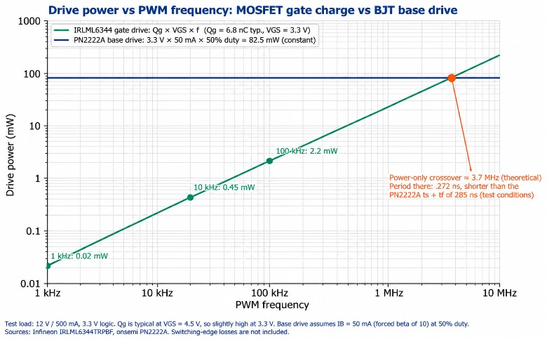
What differs is the drive cost. A MOSFET gate costs Qg × VGS × f. Using 6.8 nC (typical, measured at 4.5 V, so slightly high at 3.3 V) and 3.3 V:
| PWM frequency | MOSFET gate-drive power | BJT base-drive power (50 mA, 50% duty) |
|---|---|---|
| 1 kHz | 0.02 mW | 82.5 mW |
| 20 kHz | 0.45 mW | 82.5 mW |
| 100 kHz | 2.2 mW | 82.5 mW |
The BJT's base drive is constant, so the two curves cross near 3.7 MHz. This is a power-only crossover on paper, not a usable operating point: the period there is about 270 ns, shorter than the 285 ns of storage plus fall time listed below, and an MCU pin could not charge the MOSFET gate that fast either. The practical limits are different. A BJT is limited by storage time: the PN2222A lists ts ≤ 225 ns and tf ≤ 60 ns at IC = 150 mA and IB = 15 mA. At 100 kHz the period is 10 µs, so storage time delays turn-off by about 2% of the period and sets a minimum pulse width. At 20 kHz the same delay is under 0.5% of the period and rarely matters.
A MOSFET is limited by how fast the pin can charge the gate. Datasheet switching times assume a stiff driver, and a weak pin stretches them. A suitable driver must meet the circuit's gate-drive current and switching requirements.
Power consumption
With a forced beta of 10, a BJT needs a base current equal to about 10% of its collector current. This base current adds to the power used by the control circuit whenever the transistor is ON.
A MOSFET draws almost no DC current at its gate under steady-state conditions. However, its gate must be charged and discharged during switching, which uses energy.
For example, if a BJT needs 50 mA of base current and the load is ON for 10% of the time, the average base current is about 5 mA. This assumes the base current is 50 mA during each ON period and zero during the OFF period.
Off-state leakage can also affect power consumption, especially in battery-powered circuits. The PN2222A specifies a maximum collector-emitter cutoff current (ICEX) of 10 nA under its stated test conditions (VCE = 60 V and VEB(off) = 3 V). The IRLML6344 specifies a maximum drain-source leakage current (IDSS) of 1 µA at 25 °C and 150 µA at 125 °C, with VDS = 24 V.
These values come from different test conditions, so they are not a direct comparison. For circuits with very low standby-power requirements, check the leakage specifications across the full operating temperature range.
Summary by operating range
| Operating condition | Favors | Reason |
|---|---|---|
| Logic supply of 5 V or less, load current of 200 mA or more | Logic-level MOSFET | A typical MCU pin may not provide enough BJT base current, while a suitable MOSFET can have a low on-state voltage drop |
| Load current of 50 mA or less, with cost as the main concern | BJT or small MOSFET | Either device may work well; compare voltage drop, control requirements, and total circuit cost |
| PWM switching at 20 kHz or higher | MOSFET | A MOSFET avoids continuous base-drive current and does not have the same saturation storage-time issue as a BJT |
| Load current of 3 A or more | Suitable power MOSFET | A low on-resistance can reduce conduction loss and heat compared with a BJT that has a high saturation voltage |
These are general guidelines, not fixed rules. The best choice depends on the exact device, drive voltage, load current, switching frequency, thermal conditions, and total circuit cost
Reading Datasheets and Avoiding Selection Mistakes
BJT parameters that matter
The headline hFE hides a lot. The PN2222A lists 100 to 300 at 150 mA but only 40 minimum at 500 mA. The 2N3904's minimum falls from 100 at 10 mA to 30 at 100 mA (VCE = 1 V). Read VCE(sat) together with its IC/IB condition, VBE(sat) for drive headroom, and storage and fall time with their test conditions, which may not match your load.
MOSFET parameters that matter
Read RDS(on) at your actual VGS and at a realistic temperature. Then check Qg, Ciss, and the safe operating area (SOA) if the device will ever work in its linear region. Qg is quoted at specific VGS, VDS, and ID conditions (6.8 nC for the IRLML6344 at its 4.5 V test point), so compare parts only at matching conditions. Treating VGS(th) as a drive voltage is covered in the MOSFET switch guide.
Temperature effects
Datasheet values are usually quoted at 25 °C, and both devices drift. A silicon BJT's VBE falls by roughly 2 mV per °C, and its gain changes with temperature, as the PN2222A's hFE curves at several junction temperatures show. A MOSFET's RDS(on) rises with temperature, so conduction loss grows as the part warms, while its threshold falls (one AO3400A datasheet lists −2.82 mV/°C). Use the hot values for heat calculations, and check that a threshold shift does not leave a marginal gate drive too weak or an off state too leaky.
Curves to open first
For a BJT, open the hFE vs IC curve and the VCE(sat) vs IC curve. For a MOSFET, open RDS(on) vs VGS, RDS(on) vs temperature, and the gate-charge curve. These five graphs answer most selection questions faster than the summary table.
Side-by-side datasheet comparison
| Parameter | Question it answers | PN2222A (onsemi) | IRLML6344TRPbF (Infineon) |
|---|---|---|---|
| Type / package | What am I buying? | NPN BJT, TO-92 | N-channel MOSFET, SOT-23 |
| Maximum voltage | What can it block? | VCEO 40 V | VDS 30 V |
| Continuous current | What can it carry? | 600 mA | 5 A (TA = 25 °C) |
| Drop at 500 mA | What do I lose when on? | VCE(sat) ≤ 1.0 V (IB = 50 mA) | ≤ 18.5 mV (from 37 mΩ) |
| Gain / threshold | How is it turned on? | hFE ≥ 40 at 500 mA | VGS(th) 0.5 to 1.1 V |
| Drive requirement | What must the pin supply? | IB = 50 mA | VGS ≥ 2.5 V, IGSS ≤ 100 nA |
| Switching | How fast is it? | ts ≤ 225 ns, tf ≤ 60 ns (150 mA test) | Qg = 6.8 nC typical |
| Off-state leakage | What leaks when off? | ICEX ≤ 10 nA | IDSS ≤ 1 µA (25 °C), ≤ 150 µA (125 °C) |
Selection mistakes
- Relying on headline hFE. Use the gain listed at your collector current, and design from the forced beta in the VCE(sat) test.
- Treating VGS(th) as the turn-on voltage. It marks where conduction starts, not where RDS(on) is low.
- Comparing parts at different test conditions. The 2N7002's maximum RDS(on) near 4.5 V to 5 V differs by a factor of 2.5 between datasheets (see the crossover discussion), and the test currents differ too.
- Reading ID at 25 °C as usable current. Continuous current falls as the board and enclosure warm up.
- Using a MOSFET in its linear region without checking SOA. Slow transitions and linear operation concentrate heat in small areas.
- Treating absolute maximum ratings as operating limits. A 40 mA pin rating or a 6 V base-emitter limit is a damage threshold, not a design target.
- Choosing on unit price alone. Count drive parts, heat sinking, and rework as part of the cost.
From Decision to Part Number
Apply the workflow to the test load, a 12 V / 500 mA load on 3.3 V logic:
- Lock the load. 12 V, 500 mA, resistive. If inductive, add a clamp.
- Lock the drive. A 3.3 V pin at 20 mA or less. The BJT needs 50 mA, so it fails. The MOSFET needs VGS of 2.5 V or more, so it passes.
- Pick the device type. A logic-level MOSFET.
- Shortlist three to five parts with margin, in a package that fits the thermal budget.
- Check datasheet test conditions against your real conditions: RDS(on) at 2.5 V, VGS(max) of ±12 V, and 5 A rating against a 0.5 A load.
- Prototype and measure. Expect at most 18.5 mV across the MOSFET at 500 mA, and confirm the temperature. Also probe the logic pin under load: a BJT's base current can pull the high level down and reduce its own drive.
| Candidate | Type | Key datasheet limits | Note |
|---|---|---|---|
| IRLML6344TRPbF (Infineon) | N-channel MOSFET, SOT-23 | VDS 30 V; RDS(on) ≤ 37 mΩ at 2.5 V; VGS ±12 V | Guaranteed at 3.3 V logic |
| AO3400A (Alpha & Omega) | N-channel MOSFET, SOT-23 | VDS 30 V; ID 5.7 A at 10 V; RDS(on) < 48 mΩ at 2.5 V | Check which maker's datasheet applies |
| PN2222A (onsemi) | NPN BJT, TO-92 | IC 600 mA; VCE(sat) ≤ 1.0 V at 500 mA / 50 mA | At its limit; needs 50 mA base drive. Pinout E-B-C (P2N2222A is C-B-E) |
If two parts both pass, prefer the one whose key limits are specified at your own conditions and that has more than one source.
Record the conditions you assumed (drive voltage, temperature, test current) next to each part in the BOM. When a buyer later proposes an alternate, those conditions tell them exactly which datasheet lines to compare.
From Shortlist to Purchase: What Buyers Should Check
Inventory, MOQ, and lead time
Small-signal BJTs such as the 2N3904 and PN2222A are mature, multi-source parts, so stock is usually broad. Logic-level MOSFETs are also common but vary more by maker. SOT-23 parts commonly ship on 3,000-piece reels, so check whether smaller quantities are sold, and whether the minimum order quantity differs from the standard package quantity. Lead time varies by package and manufacturer, so confirm it per part number and ask whether stock is on hand or on order. Ask for stock by manufacturer, not just by part number, since one part number may be offered from several makers.
Unit price and volume pricing
Compare the cost of the whole circuit, not unit price alone. A BJT circuit may add a pre-driver and resistors, while a MOSFET circuit adds a gate resistor and pull-down. Check price breaks at your volume, since the cheapest part at one quantity may not be cheapest at another. Price breaks often fall at reel multiples, so a small increase in order size can lower the unit price.
Package and manufacturer
Name the manufacturer in the BOM, and keep an approved alternate list with the conditions under which each alternate was checked. Datasheets carrying the AO3400A name list maximum RDS(on) at 2.5 V anywhere from 24 mΩ to 52 mΩ, depending on the maker. TO-92 pin order is not standardized, even within one family. onsemi's PN2222A is E-B-C (emitter, base, collector), while its P2N2222A is C-B-E, so the wrong variant in the same footprint will not switch correctly and can be damaged. Check the pinout in the datasheet of the exact part number before substituting.
Lifecycle, RoHS, and automotive-grade (AEC-Q101)
Check each manufacturer's lifecycle status (active, not recommended for new designs, or obsolete). Classic BJT types have many sources, but the exact variant from a given maker can still change status, and newer MOSFET series are updated more often. Confirm RoHS on the datasheet, or request the manufacturer's declaration if it is not stated. For automotive use, qualified variants often carry a different prefix or suffix (onsemi uses a 2V prefix on its 2N7002K family), so confirm AEC-Q101 qualification on the datasheet, not from the name.
Authorized sourcing and counterfeit risk
High-volume commodity parts can be relabeled or substituted. Buy from authorized channels, or verify independent lots by incoming inspection. Ask for the manufacturer's certificate of conformance, and check that the lot and date codes, markings, and packaging are consistent. Unikeyic lists its authorized line card and quality control process for reference.
When you are ready, search by part number or filter by parameters in the Unikeyic product catalog, check in-stock parts, and send a quote request for volume pricing.
FAQ
Can a MOSFET replace a BJT directly?
Not directly. A MOSFET is driven by gate voltage and a BJT by base current, so the drive network must be redesigned, and the pin order must be checked. See the switching section.
Is a MOSFET always better for switching?
No. At low current a small MOSFET and a BJT can have similar drops, and a BJT may cost less. For loads within the pin's base-current limit, a BJT is a legitimate choice. See the low-current crossover and the lighter-load example.
Can I drive either one directly from an Arduino pin?
A logic-level MOSFET, yes, at modest frequency. A BJT only if its base current stays within the pin limit, which caps the load it can carry. See operating limits.
Which is better for audio amplification?
It depends on source impedance and noise needs: BJTs suit low-impedance sources, MOSFETs high-impedance ones. See the amplifier section.
Do both devices need flyback protection?
Yes, on inductive loads such as coils and motors. The same diode or clamp works for both devices. See the switching section.
Which is cheaper, and which handles heat better?
Price depends on part and volume, so compare total circuit cost. At the same current, a MOSFET usually dissipates less. See operating limits and the purchase section.
Conclusion
Three rules cover most decisions. First, check what the pin can supply: a BJT needs about one-tenth of the load current as base current. Second, compare on-state drop at your own current and drive voltage, using datasheet limits, not rules of thumb. Third, name the manufacturer and confirm availability before the design is frozen, because the same part number can carry different limits from different makers.
Datasheets give the limits, but only a prototype confirms them. Measure the drop, the temperature, and the pin voltage under load before releasing the design.
When the shortlist is ready, browse the Unikeyic catalog to check stock and pricing.