PMOS High-Side Switch Circuit Design Guide
Designing a p-channel MOSFET high-side switching circuit involves more than selecting a p-channel MOSFET. You need to understand how the microcontroller's GPIO signal controls the gate driver, how the driver switches the PMOS, and how the PMOS supplies power to the load.
In this guide, we'll design a practical GPIO-controlled PMOS high-side switch circuit from start to finish. We'll look at how to connect the GPIO, choose and position the driver transistor, select the PMOS and its protection components, and calculate the required resistor and Zener diode values. We'll also examine how to connect the load, protect the circuit from inductive voltage spikes, and ensure the components operate within their electrical and thermal limits.
How Does a P-channel MOSFET Work As a High-Side Switch
High-side switching is a method of controlling power to a load by placing the switch between the positive power supply and the load. The other end of the load remains connected to ground. So, we have the MOSFET connected between the power supply and the load; the other end of the load connects to the ground.
When the switch is ON, current flows from the power supply through the switch and load to ground. When it is OFF, the switch cuts off the positive supply to the load.
There are two common ways to switch power to a load:
-
High-side switching: The switch is placed between the positive supply and the load.
-
Low-side switching: The switch is placed between the load and ground.
P-channel MOSFETs are commonly used for high-side switching because they turn ON when the gate voltage is sufficiently lower than the source voltage and turn OFF when the gate returns close to the source voltage.
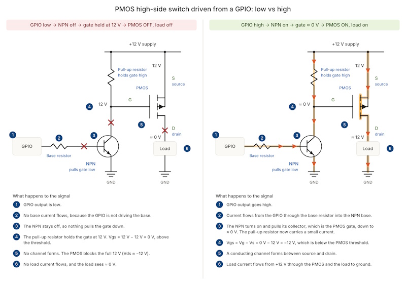
This PMOS arrangement is one of the three common MOSFET switching topologies, alongside N-channel low-side switching and driver-assisted N-channel high-side switching.
Where are PMOSFET high-side switches used?
High-side switching is useful in applications such as automotive electronics and battery-powered devices, where controlling the positive supply to a load is important.
Table 1: Common applications of PMOSFET high-side switching
|
Application |
Example |
|---|---|
|
Battery-powered devices |
Turning sensors or other circuit sections ON and OFF |
|
Automotive electronics |
Switching power to electronic modules |
|
Industrial control systems |
Controlling power to sensors and control circuits |
|
Power management circuits |
Enabling or disabling different power rails |
|
Load switching |
Controlling power to motors, LEDs, and other loads |
How To Design a PMOSFET High-Side Switching Circuit?
Let us see how to design a complete PMOS high-side switching circuit. We will discuss how to choose the PMOS for the application and study the different parameters to consider. Here’s a quick checklist of these parameters:
Here’s a parameter checklist when selecting your PMOSFET:
-
VDS: Can it withstand the maximum voltage in your circuit?
-
VGS: Can it safely handle the gate-to-source voltage?
-
ID: Can it carry the required current?
-
RDS (on): Will the power loss and heat be acceptable?
-
VGS (th): At what gate voltage does it begin conducting?
-
Switching characteristics: Can it switch at the required speed?
-
Package: Can the package dissipate the heat?
Drain-to-source voltage (VDS)
Suppose your circuit uses a 12 V supply, with a maximum expected operating voltage of 13.2 V. You need a PMOS whose VDS rating is comfortably above 13.2 V. You should also give an additional allowance for voltage spikes.
As a general rule of thumb, you can choose a VDS rating at least 20% above the maximum operating voltage. However, the actual margin depends on the circuit and its transient conditions.
Gate-to-source voltage (VGS)
Step 1: Check the maximum VGS rating
VGS is the voltage difference between the gate and the source terminals. It determines whether the MOSFET turns ON or OFF. It also gives an idea about how much voltage the gate can safely handle.
VGS = VG - VS
-
Check the maximum VGS rating in the datasheet
Every P-type MOSFET has a maximum gate-to-source voltage it can handle. This is usually listed as VGS(max) in the datasheet.
For example, suppose a PMOS has a maximum VGS rating of ±12 V. This means the voltage difference between its gate and source must not exceed 12 V in either direction.
Let's use a 12 V high-side switching circuit:
-
Source voltage: 12 V
-
Gate voltage: 0.2 V
The resulting gate-to-source voltage is:
VGS = 0.2 - 12 = -11.8 V
The PMOS turns on because its gate is at a lower potential than its source. However, we can see that -11.8 V is very close to the source voltage of 12V. Suppose the source voltage increases suddenly to 13.2V while the gate remains at 0.2 V,
VGS = 0.2 - 13.2 = -13 V
The VGS value in this case exceeds the maximum allowable value given in the datasheet (12V), so it can damage the MOSFET. So always choose a MOSFET whose maximum VGS rating comfortably accommodates the voltage your gate-drive circuit can produce.
There are two solutions to protect your MOSFET from excessive gate voltage:
-
Use a Zener diode: Use a suitably selected Zener diode between the gate and source to clamp excessive voltage. A Zener diode limits the voltage difference between these two terminals. If VGS tries to exceed the Zener's breakdown voltage, the diode conducts and clamps the voltage. For example, a suitable 15 V Zener can limit the magnitude of VGS to approximately 15 V under the intended operating conditions. The Zener diode voltage should be high enough to allow the required gate drive but low enough to protect the gate.
-
Use a dual-resistor voltage divider: A voltage divider uses two resistors to reduce the voltage applied to the gate.
VG = VCC × (R2/ (R1+R2))
Suppose the system uses a 24V supply and two 10 kΩ resistors:
VG = 24 × (10k/ (10k+10k)) = 12V
The gate is therefore at 12 V while the source is at 24V.
VGS = 12 - 24 = -12V
This keeps the gate-source voltage within the example MOSFET's ±20 V rating.
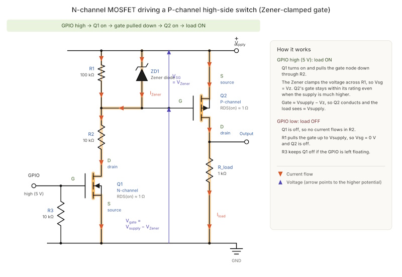
Step 2: Check the VGS required for fully turning ON the MOSFET
The maximum VGS rating tells you how much voltage the gate can safely handle. But it doesn't tell you how much voltage is needed to turn the MOSFET ON efficiently.
For this, check the RDS (on) specifications in the datasheet.
Table 2: RDS (on) value examples
|
VGS |
RDS(on) |
|---|---|
|
-10V |
11 mΩ |
|
-4.5V |
14 mΩ |
Table 2 tells you that the MOSFET has a guaranteed maximum ON-resistance of 14 mΩ when VGS is -4.5 V, and 11 mΩ when VGS is -10 V, under the datasheet's specified test conditions. Suppose your gate driver can only produce -4.5 V. You should check whether the corresponding RDS (on) is low enough for your load current and thermal requirements.
Note: Don't confuse gate threshold voltage (VGS(th)) with the voltage needed for full turn-on. VGS(th) only indicates when the MOSFET begins conducting a small amount of current. It does not guarantee low ON-resistance.
Step 3: Consider the gate-drive circuit
Your gate-drive circuit must produce the correct VGS without exceeding the MOSFET's maximum rating.
For example, consider a 12 V supply controlled by a 3.3 V microcontroller.
Connecting the microcontroller directly to the PMOS gate may not be suitable. When the GPIO outputs 3.3 V, the gate is still significantly below the 12 V source, so the PMOS may remain partially or fully ON instead of switching OFF.
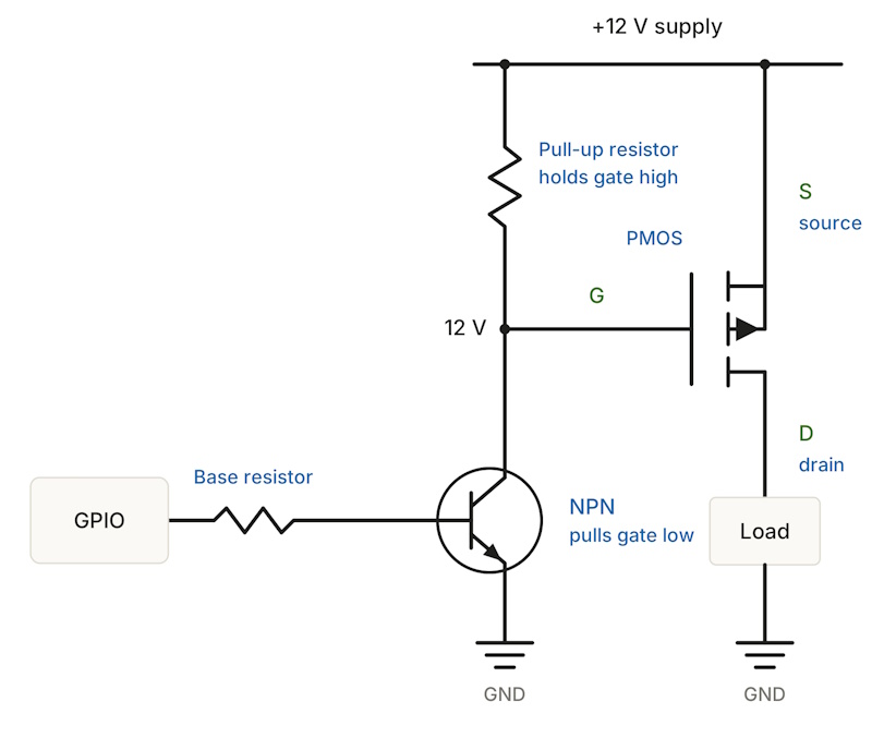
The solution? Use an NPN transistor or an NMOS transistor as a gate driver. This allows the circuit to pull the PMOS gate towards ground when switching ON. It can also pull it back towards the source voltage when switching OFF. We have discussed this in detail in the practical example at the end.
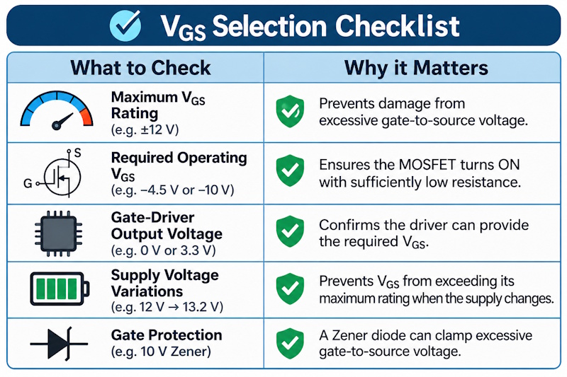
Summary
Check both the maximum VGS rating and the VGS required to achieve the specified RDS(on). The gate driver must provide enough negative voltage to turn the PMOS ON efficiently, while keeping that voltage within the MOSFET's safe operating limits.
Current rating, ID
ID is the drain current rating. It tells you how much current the MOSFET can carry under the manufacturer's specified test conditions. But a MOSFET rated for 5 A can not continuously handle 5 A in your circuit. Its actual current-handling capability also depends on power loss and temperature.
Let's say your load normally draws 2 A, and you've selected a PMOS with a maximum drain current rating of 5 A. Before using it, check the following:
1. Check the power dissipation
The RDS(on) value can be taken from the MOSFET's datasheet, where it is specified under particular gate-to-source voltage (VGS) and temperature conditions. Let’s take it as 50 mΩ for this example. When current flows through the MOSFET, its ON-state resistance (RDS(on)) causes power loss. You can estimate this using:
Pcond = IDS2 × RDS
= 22 × 0.05 = 0.2W
This means the MOSFET dissipates approximately 0.2 W as heat due to conduction.
2. Estimate the Junction Temperature
The datasheet provides two thermal resistance values, as seen in Table 3.
Table 3: PMOSFET thermal resistance values (Example)
|
Parameter |
Value |
What it tells you |
|---|---|---|
|
RθJA |
420C/W |
Temperature rise from the junction to the surrounding ambient air |
|
RθJC |
120C/W |
Temperature rise from the junction to the case |
For a typical PCB-mounted design, you can use RθJA to estimate the junction temperature:
TJ = TA + (P ×RθJA)
Where:
-
TJ : Junction temperature
-
TA: Ambient temperature
-
P: Power dissipated by the MOSFET
Compare this value with the maximum junction temperature specified in the datasheet. It should remain below that limit under expected operating conditions.
The RθJC value is useful when you can measure or estimate the MOSFET’s case temperature. In this case, use:
TJ = TC + (P ×RθJC)
For example, if the case temperature is 400C and the MOSFET dissipates 0.2W:
TJ = 40 + (0.2 × 12) = 42.40C
Note: Thermal resistance values depend on the test conditions and PCB arrangement. The actual junction temperature can be higher if the board has limited copper area, poor heat dissipation, or a high ambient temperature. Also, the calculations above consider conduction loss only. Include switching losses if they are significant in your application.
3. Check startup and peak current
Some loads draw more current when they first turn on. For example, a motor that normally draws 2 A may need considerably more current during startup.
-
It’s not enough to only the motor's normal operating current. You also need to find its startup or stall current from the motor datasheet, or measure it in the actual circuit.
-
Next, check whether the MOSFET can handle that current for the required duration. Look at its pulsed drain current rating and Safe Operating Area (SOA), along with the relevant pulse-duration and thermal limits. A MOSFET that can handle a brief current peak may not be suitable for carrying the same current continuously.
-
If the startup current is too high, consider a suitable current-limiting circuit or motor driver. For capacitive loads, a soft-start or inrush-current-limiting circuit can help reduce the initial current surge.
Switching characteristics
A MOSFET doesn't turn ON or OFF instantly. Even after applying a gate signal, it takes some time for the device to change its operating state.
This transition is described using four important datasheet parameters:
-
Turn-on delay time (td(on)): Turn-on delay time is the time between applying the turn-on signal to the MOSFET gate and the beginning of the drain current response. A MOSFET with a shorter turn-on delay can respond faster, assuming comparable test conditions and gate-drive circuits.
-
Rise time (tr): Rise time is the time taken by the drain current to increase from approximately 10% to 90% of its final value during turn-on. During this transition, the MOSFET is not yet fully ON. A longer rise time can mean greater switching losses, particularly when the MOSFET is switched frequently. A shorter rise time generally helps reduce these losses, although excessively fast switching can create ringing and electromagnetic interference.
-
Turn-off delay time (td(off)): it tells you how long the MOSFET takes to start responding to an OFF command. In high-frequency applications, turn-off delay contributes to switching losses.
-
Fall time (tf): Fall time is the time taken by the drain current to decrease from approximately 90% to 10% of its initial value during turn-off. A shorter fall time can help reduce switching losses. However, with inductive loads such as motors, current may continue flowing through a flyback or recirculation path even after the MOSFET turns OFF.
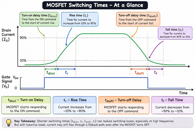
Suppose you're comparing two P-Channel MOSFETs as seen in Table 3.
Table 4: Comparing delay times of two MOSFETs (Example)
|
Parameter |
Mosfet A |
Mosfet B |
|---|---|---|
|
Turn-on delay (td(on)) |
15 ns |
25 ns |
|
Rise time (tr) |
20 ns |
35 ns |
|
Turn-off delay (td(off)) |
40 ns |
55 ns |
|
Fall time (tf) |
25 ns |
45 ns |
MOSFET A has shorter switching times across all four parameters. But it does not necessarily make MOSFET A is a better choice. You also need to consider:
-
RDS(on)
-
Gate charge (Qg)
-
VDS rating
-
VGS rating
-
Current rating
-
Thermal performance
For example, a MOSFET with excellent switching times but high RDS(on) might generate more conduction losses. You need to consider the complete set of requirements given above.
Do switching times matter equally in every application? No. This is particularly important when selecting a MOSFET.
For applications like PWM motor control or a high-frequency power supply where the MOSFET switches repeatedly, even small differences can influence total switching losses. Now suppose you're designing a battery-powered sensor that switches ON for 10 seconds and OFF for 10 seconds. A difference of 10 to 20 nanoseconds in switching time may not make much difference to the overall application.
Note: Datasheet switching times are measured under specific test conditions, such as VDS, VGS, gate resistance (RG), and load resistance (RL). Always compare MOSFETs using switching times measured under similar test conditions.
Gate Charge, Miller Charge, and Input Capacitance
When selecting a MOSFET, you need to understand how much charge the gate driver must supply or remove to switch the device. Three useful datasheet parameters are total gate charge (QG), gate-drain charge (QGD), and input capacitance (Ciss).
1. Total Gate Charge (QG)
QG indicates the total charge required to switch the MOSFET under specified test conditions. A higher QG generally means the driver needs to supply more charge. This can increase switching time if the driver has limited current capability.
2. Gate-Drain Charge (QGD)
QGD is the charge associated with the Miller plateau. During this stage, the gate voltage changes very little while the drain-to-source voltage changes significantly.
Let's understand this using the gate-charge curve in Figure 6.
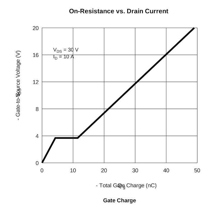
The curve has three regions:
-
Initial charging: The gate voltage increases as the driver supplies charge. The MOSFET starts turning ON.
-
Miller plateau: The gate voltage remains almost constant while additional charge is supplied. This charge is associated with Qgd.
-
Final charging: The gate voltage increases again until it reaches the required drive voltage.
For example, in the illustrated curve in Figure 6, the Miller plateau extends approximately from 5 nC to 12 nC. Therefore, QGD is approximately 7 nC.
You can use this curve to understand how much charge the driver must supply during switching. A higher Qgd generally means more time is needed for the drain voltage transition, assuming the same gate-drive current.
3. Input Capacitance (Ciss)
Ciss represents the input capacitance seen by the gate driver. It is approximately the sum of gate-source capacitance (CGS) and gate-drain capacitance (CGD).
However, Ciss varies with the drain-to-source voltage and cannot fully describe the charge required during switching. Therefore, use it as a supporting parameter rather than the primary indicator of gate-drive requirements.
When comparing MOSFETs, check QG, QGD, and the gate-charge curve under similar datasheet test conditions. Also consider whether your gate driver can supply sufficient current to switch the MOSFET within the required time.
For simple ON/OFF switching, extremely fast switching may not be necessary. However, for PWM and high-frequency applications, you may need to give more importance to gate charge and Miller charge.
Inductive load protection: When to use a flyback diode in a high-side switching circuit
The PMOS can be used to switch inductive loads like motors, relay coils, solenoids, and actuators. These loads contain coils that store energy in a magnetic field while current flows through them. When the MOSFET switches OFF, the current through the coil cannot stop instantly. The collapsing magnetic field produces a voltage spike. This spike can become high enough to damage the MOSFET.
A freewheeling diode provides a path for the stored energy to circulate after the MOSFET switches OFF. It is also called a flywheel or flyback diode.
The diode is connected across the load:
-
Anode: Connected to the MOSFET drain side of the load.
-
Cathode: Connected to the positive supply (VCC).
During normal operation, the diode is reverse-biased and does not conduct. When the MOSFET switches OFF and the load generates a voltage spike, the diode provides a path for the current.
How to choose the flywheel diode
Consider two parameters while choosing the flywheel diode:
-
Reverse voltage rating (VRRM): Must withstand the voltage across the diode. It should be at least 1.5 times the supply voltage.
-
Current rating: Should be greater than the load current.
The diode must also be suitable for the switching frequency and operating conditions. Please note that a purely resistive load, such as a heater, does not store magnetic energy, so a flywheel diode is not required.
PMOS High-Side Switch: Complete Design Through Practical Example
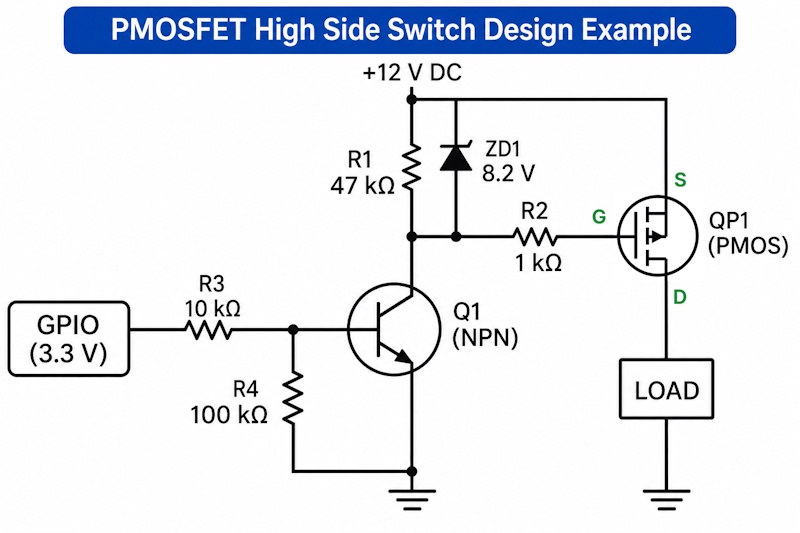
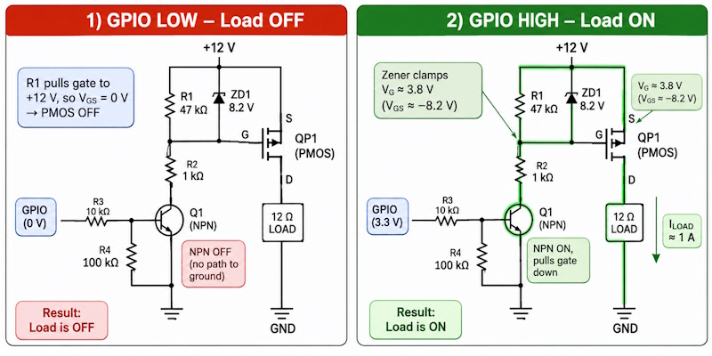
Let us design a complete high-side switch using PMOS. First, let’s make a list of the design requirements, as seen in Table 5.
Table 5: High-side PMOS switching circuit design requirements
|
Parameter |
Design requirement |
|---|---|
|
Supply voltage |
12 V DC |
|
Microcontroller output |
3.3 V |
|
Load |
Resistive |
|
Load resistance |
12 Ω |
|
Load current |
1 A |
|
Switching type |
High-side |
|
Control device |
NPN BJT |
|
Main switch |
P-channel MOSFET |
Now we will design each of these parameters. We cannot connect the GPIO pin directly to the PMOS gate.
If we connect the GPIO directly to the PMOS gate:
-
GPIO HIGH = 3.3 V, giving VGS = 3.3 - 12 = -8.7V. The PMOS turns ON.
-
GPIO LOW = 0 V, giving VGS = 0 - 12 = -12V. The PMOS also remains ON.
Both GPIO states could leave the PMOS ON, so an additional circuit is required to control the gate correctly. This is why the design uses an NPN transistor as a discrete gate driver and level shifter; the broader gate-driver architecture and selection criteria also depend on drive voltage, gate charge, source and sink current, switching time, and isolation requirements.
Why use an NPN transistor in a PMOS switch circuit
The NPN transistor acts as a switch that controls the PMOS gate. The NPN transistor acts as an electrically controlled path to ground.
-
When the NPN is OFF, it does not provide a conducting path from collector to emitter.
-
When the NPN is ON, it provides a low-resistance path between collector and emitter.
This allows us to pull the PMOS gate down when required. For our example, you can use a BC547, but check its pinout and electrical ratings.
Designing resistor R3 for PMOS high-side switch circuit
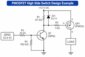
The GPIO connects to the NPN base through resistor R3, which is a 10 kΩ resistor. The base-emitter junction behaves approximately like a forward-biased diode. Without a resistor, connecting 3.3 V directly to the base could cause excessive current to flow from the GPIO. We therefore limit the base current (IB).
IB = (VGPIO - VBE)/RB
IB = (3.3 - 0.7)/10000 = 0.26mA
The 10 kΩ resistor provides adequate base drive while consuming less GPIO current.
Designing resistor R4 for PMOS high-side switch circuit
R4 is the base pull-down resistor. It connects the NPN base to ground (through its emitter). It keeps the NPN OFF when the microcontroller GPIO is floating, such as during startup or reset. Without it, electrical noise could accidentally turn the NPN ON. For this design, 100 kΩ is a reasonable choice.
Designing Gate-to-source pull-up resistor R1 (47 kΩ)
A MOSFET gate is insulated. It does not have a normal DC path that reliably establishes its voltage by itself. If the gate is left floating, its voltage can become unpredictable. We need to establish a defined OFF state through the 47 kΩ resistor.
When the NPN is off, the resistor R3 pulls the PMOS gate towards its source voltage.
VG = 12V
VS = 12V
VGS = 12-12 = 0V
The PMOS is OFF.
We don’t have a fixed universal formula to calculate the value of R1. You can consider these factors while selecting the resistor:
-
The desired gate discharge/charge time.
-
The MOSFET gate charge and capacitance.
-
The acceptable static current.
-
The gate driver's ability to pull the gate down.
For our example, we select 47 kΩ as a practical starting value.
Let's calculate the current through it when the PMOS is ON, and the Zener clamps the gate at approximately 3.8 V.
IR4 = (12 - 3.8) / 47000 = 0.174 mA
This is a small current.
A higher resistance would reduce this current but could increase turn-OFF time. A lower resistance would provide a stronger pull-up but increase the current that the NPN must sink.
How to choose the Zener diode for PMOS high-side switching circuit
The Zener diode protects the PMOS gate, as we discussed in the previous sections.
It is important to know how to connect the Zener diode in the circuit:
-
Cathode (K) → PMOS Source (+12 V).
-
Anode (A) → PMOS Gate.
We need to consider two things while selecting the voltage for the Zener diode:
-
The Zener voltage must be below the MOSFET's maximum gate-source voltage, including tolerance and transients.
-
It must still provide sufficient gate drive to turn the PMOS fully ON.
For a MOSFET rated at ±20 V, an 8.2 V Zener is a reasonable choice for this 12 V example. When the Zener enters breakdown, it maintains approximately 8.2 V between the PMOS source and gate. Therefore, the gate voltage is:
VG = Vs - Vz = 12 - 8.2 = 3.8V
VGS = 3.8 - 12 = -8.2 V
This means the Zener limits the magnitude of the negative gate-to-source voltage to approximately 8.2 V, protecting the MOSFET from excessive gate voltage.
We could use a different Zener voltage depending on the selected MOSFET and supply conditions. For this example, select an 8.2 V, 0.5 W Zener diode.
Designing R2: Zener current-limiting resistor
R2 connects the PMOS gate to the NPN collector. When the NPN turns ON, the Zener enters breakdown and conducts current. If we connect the NPN collector directly to the gate without a current-limiting element, excessive current could flow through the Zener. The resistor R2 limits this current.
R2 = (VSUPPLY - VZ - VCE (sat))/IC
R2 = (12 - 8.2 - 0.2)/0.0036 = 1kΩ
The power dissipated in this resistor is approximately:
P = I2R
P = (0.0036)2 ×1000 = 0.013W
A standard 0.125 W or 0.25 W resistor is sufficient.
How To Design The PMOS for a High-Side Switch Circuit
We have a 12 Ω resistive load.
Using Ohm's law:
ILOAD = V/R = 12/12 =1A
The PMOS must be able to handle this current.
For example, if the selected MOSFET has an ON resistance of 30 mΩ at the actual gate drive:
PMOSFET = ID2 RDS (on)
PMOSFET = 12 × 0.03 = 30mW
This is its approximate conduction loss. Thermal design must also consider the actual PCB layout, ambient temperature, and switching losses.
Load current is only one selection criterion. After defining the required VDS, ID, RDS(on), VGS, gate charge, package, and thermal limits, compare suitable N-channel and P-channel MOSFETs against the complete set of circuit requirements.
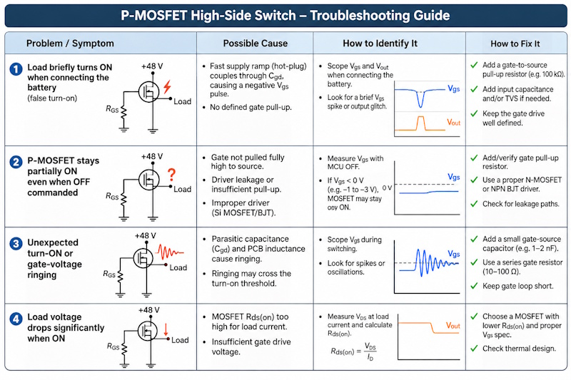
At times, the completed circuit may not work as intended. For example, the PMOS may stay ON even when it is supposed to stay OFF, or the load voltage may drop significantly. Use the PMOS high-side switch troubleshooting guide given in Figure 8 to fix these common problems.
When To Choose Power MOSFETs For High-Side Switching
We just discussed the importance of adding separate gate driver circuits for PMOS high-side switching circuits. Some motor driver ICs, such as the TMC2300, have power MOSFETs and their associated gate-drive circuitry integrated into a single chip. This offers several advantages, such as:
-
Simpler circuit design
-
Compact size
-
Low ON resistance
-
Coordinated switching
When Should You Choose an Integrated Driver?
An integrated motor driver is ideal when designing compact applications such as stepper motor controllers, printers, robotics, and battery-powered equipment. It reduces component count and simplifies gate-drive and switching control.
On the other hand, discrete power MOSFETs with external gate drivers offer greater flexibility when designing circuits that require higher currents, different voltage ratings, customised switching arrangements, or greater control over component selection.

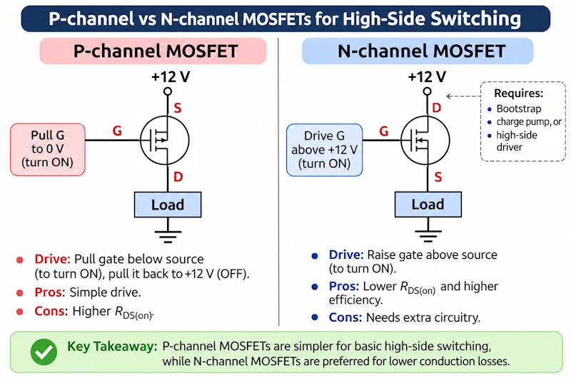
P-channel vs n-channel MOSFETs for high-side switching: What is the difference?
Both P-channel and N-channel MOSFETs can serve as high-side switches, but their gate-drive requirements, conduction losses, and topology constraints determine which device is the better fit.
-
P-channel MOSFET: Easier to drive because its gate can be pulled below the source voltage to turn it ON. However, it generally has higher ON-resistance, resulting in greater conduction losses.
-
N-channel MOSFET: Generally offers lower ON-resistance and better efficiency. However, its gate must be driven above the source voltage, requiring a dedicated high-side driver, bootstrap circuit, or charge pump.
Isolation and Grounding When Connecting an MCU to a P-Channel MOSFET
When controlling a p-channel MOSFET using an MCU, the grounding arrangement matters. The MCU generates the control signal, while the MOSFET switches power to the load. If both circuits share ground, the current flowing through the load circuit can introduce unwanted noise into the MCU's ground reference.
For example, consider a 24 V solenoid controlled by an MCU operating at 3.3 V. When the solenoid switches ON and OFF, its current flows through the power circuit. Suppose the load current and MCU return current share PCB traces or ground paths. The voltage drops and switching noise can affect sensitive MCU signals, including sensor readings.
One easy solution is to keep load and control current paths separate.
-
Route the solenoid's return current through a dedicated path to the power supply ground.
-
Route the MCU's ground return separately.
-
Bring the ground connections together at a carefully selected common point, such as a star-ground connection near the driver.
If you want true electrical isolation, you must isolate both the control signal and its power supply. Isolating only the ground connection may not be sufficient.
When should you use an optocoupler?
An optocoupler can transfer the MCU's control signal to the MOSFET-driving circuit without a direct electrical connection between the two sides.
However, the isolation must be maintained across both the signal and power connections. The driver side needs its own isolated power supply, too.
You can consider this approach when the design requires electrical isolation between the control and power circuits. It is not automatically necessary just because the load current is high or switching noise is present.
FAQs
Can an n-channel MOSFET be used as a high-side switch?
Yes. An n-channel MOSFET can be used as a high-side switch, but its gate voltage must be higher than its source voltage by the required VGS to turn ON.
Since the source voltage rises towards the supply voltage when ON, the gate must be driven above the supply voltage. This typically requires a bootstrap circuit, charge pump, or dedicated high-side gate driver.
How does a p-channel MOSFET work as a switch?
A p-channel MOSFET switches ON and OFF based on its gate-to-source voltage (VGS).
-
OFF: When the gate and source are at approximately the same voltage (VGS = 0).
-
ON: When the gate is pulled sufficiently below the source, making VGS negative.
For example, in a 12 V circuit, pulling the gate to 0 V gives VGS = - 12V turning the MOSFET ON, provided this is within its voltage rating.
How do you drive a high-side MOSFET?
The gate-drive method depends on the MOSFET type:
-
P-channel MOSFET: Pull the gate below the source to turn it ON and back up to the source voltage to turn it OFF. A transistor-based level shifter can provide this control.
-
N-channel MOSFET: Drive the gate above the source voltage to turn it ON. This typically requires a bootstrap circuit, charge pump, or dedicated high-side gate driver.
The driver must provide the required gate voltage and sufficient current to charge and discharge the gate at the desired switching speed.
What is a high-side switching MOSFET?
A high-side switching MOSFET is connected between the positive power supply and the load. It controls the power supplied to the load.
When ON, current flows from the supply through the MOSFET and load to ground. When OFF, it interrupts the current flow.