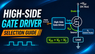
High-Side Gate Driver Selection Guide
Table of Contents
- What Is a High-Side Gate Driver?
- Define the Power Device and Circuit Topology
- Determine the Voltage Requirements
- Choose the High-Side Supply Method
- Check Duty Cycle and Bootstrap Refresh
- Evaluate Drive Current and Timing
- Evaluate Transient Robustness and Isolation
- Check Protection and Operating Requirements
- High-Side Gate Driver Selection Workflow
- Practical Selection Example: 400 V Half-Bridge with SiC MOSFETs
- Step 1: Verify the Bus Voltage and Power Device
- Step 2: Determine the Required Gate-Drive Voltage
- Step 3: Estimate the Required Gate-Drive Current
- Step 4: Evaluate Common-Mode Transient Immunity
- Step 5: Select the High-Side Supply Method
- Step 6: Check Protection and Timing
- Selection Outcome
- Datasheet Parameter Checklist
- Frequently Asked Questions
- Can a bootstrap high-side gate driver operate at 100% duty cycle?
- Is a high-side driver's voltage rating the same as its gate-drive voltage?
- Do all high-side gate drivers require isolation?
- Can the same driver be used for silicon MOSFETs and GaN devices?
- Is higher gate-driver current always better?
- What should be checked first when comparing high-side drivers?
- Conclusion
- References
Choosing a high-side gate driver requires more than matching the driver's voltage rating to the DC bus. The selected gate driver IC must provide the correct gate-drive voltage, maintain its floating supply throughout the switching cycle, and control the power device without unwanted turn-on or timing errors.
A driver that works well in a conventional PWM converter may not support continuous high-side conduction. Similarly, a driver with sufficient output current may still be unsuitable for a fast switching SiC MOSFET or GaN device if its transient immunity, supply range, or protection functions are inadequate.
This guide explains how to select a high-side gate driver based on the power device, circuit topology, operating voltage, supply method, duty cycle, switching performance, and protection requirements. The goal is to help engineers and purchasing professionals narrow down suitable components and verify their suitability against the manufacturer's datasheet.
What Is a High-Side Gate Driver?
A high-side gate driver is an integrated circuit that controls an external power transistor positioned between the positive supply rail and a load or switching node. It provides the appropriate gate-drive voltage and current while accommodating changes in the transistor's source or emitter potential. For a broader overview of gate-driver operation and types, see our gate driver selection guide.
Unlike a ground-referenced driver, a high-side driver must operate with an output reference that can rise toward the DC bus voltage. This difference directly affects the driver's supply arrangement, voltage ratings, and transient performance.
Why High-Side Driving Requires a Floating Reference
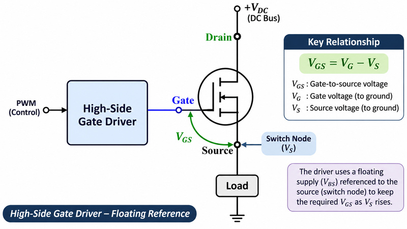
For an N-channel MOSFET, the important control voltage is the gate-to-source voltage, not the gate voltage relative to system ground.
The relationship is:
Where:
-
VGS is the gate-to-source voltage.
-
VG is the gate voltage relative to system ground.
-
VS is the source voltage relative to system ground.
When the high-side MOSFET turns on, its source voltage rises. The gate voltage must rise with it to maintain the required VGS. For example, if the source approaches 100 V and the MOSFET requires a 10 V gate-to-source drive, the gate must reach approximately 110 V relative to system ground.
The driver therefore needs a floating output stage referenced to the switching node. Depending on the application, this can be achieved through a bootstrap circuit, a charge pump, or a separate floating bias supply.
High-Side Gate Driver vs. Smart High-Side Switch
A high-side gate driver and a smart high-side switch are different product categories.
A high-side gate driver controls an external MOSFET, IGBT, SiC MOSFET, or supported GaN transistor. The designer selects the power semiconductor separately and must ensure that the driver provides the necessary voltage, current, timing, and protection.
A smart high-side switch integrates the power switching component into the device, often with load current sensing, thermal protection, and diagnostic functions. These components are commonly used for controlled load switching, including automotive applications.
This guide focuses on gate driver ICs for external power devices, including MOSFET gate drivers. Smart high-side switches should not be treated as interchangeable alternatives during driver selection.
Define the Power Device and Circuit Topology
Before comparing gate driver ICs, identify the power semiconductor and the circuit in which it operates. These choices determine the required gate voltage, gate charge, drive current, output configuration, and switching performance.
Match the Driver to MOSFET, IGBT, SiC, or GaN
Different power devices have different gate-drive requirements.
| Power device | Key driver-selection considerations |
|---|---|
| Silicon MOSFET | Gate voltage range, total gate charge, switching frequency, and suitable source/sink current |
| IGBT | Gate-to-emitter voltage, turn-off behavior, gate charge, and short-circuit protection |
| SiC MOSFET | Positive and potentially negative gate bias, fast switching, transient immunity, and protection response |
| GaN device | Tightly controlled gate voltage, low parasitic inductance, fast timing, and device-specific compatibility |
For silicon MOSFETs, the recommended gate-drive voltage depends on the selected transistor. Some are designed for conventional 10 V gate drive, while logic-level devices may operate at lower voltages. IGBTs commonly use a positive gate-to-emitter drive around 15 V, although the required values depend on the device and application [8].
Silicon Carbide (SiC) MOSFETs may require higher positive gate voltages and a negative turn-off bias. The exact gate-drive requirements of a SiC MOSFET must be checked against its datasheet [8]. GaN transistors often have a narrower allowable gate-voltage range. Certain enhancement-mode GaN transistors use a regulated drive near 5 V, making voltage accuracy particularly important [9].
A driver should never be selected based on semiconductor technology alone. Its output-voltage range, turn-off capability, timing, and protection behavior must match the specific power device.
Choose Single High-Side or Half-Bridge Configuration
The next decision is whether the application requires only a high-side output or coordinated high-side and low-side control. A single high-side driver may be appropriate for a standalone high-side switch or a converter topology in which the complementary switching device is controlled separately.
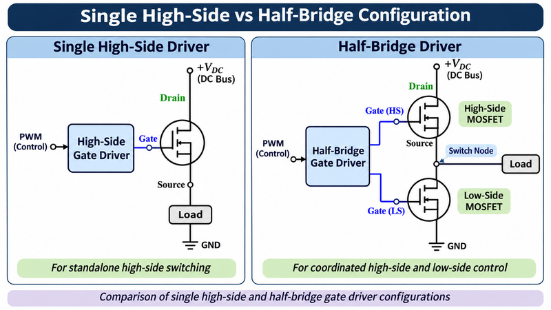
A half-bridge driver integrates high-side and low-side gate-drive channels. This arrangement is commonly used in motor drives, DC-DC converters, and inverter legs. Half-bridge drivers can simplify the circuit by combining level shifting, gate-drive outputs, and sometimes dead-time control or interlock protection.
However, the integrated configuration must support the required switching sequence. A half-bridge driver is not automatically suitable for every circuit that contains a high-side switch, especially when independent channel control or an unusual startup sequence is required.
Determine the Voltage Requirements
The driver's high-voltage capability and its gate-drive supply rating are separate specifications. Both must be checked before moving to duty-cycle or switching-performance calculations.
Bus Voltage and High-Side Voltage Rating
Start with the maximum DC bus voltage, including operating tolerance and expected transients. The driver must tolerate the voltage experienced by its high-side switching-node connection. In a bootstrap half-bridge driver, this is commonly represented by the VS or HS pin. The maximum switch-node voltage may exceed the nominal bus voltage because of ringing, switching overshoot, or other operating conditions.
Check the following datasheet parameters:
-
Maximum high-side or switch-node operating voltage
-
Absolute maximum voltage ratings
-
Permitted negative switch-node excursions
-
High-side supply-to-switch-node differential ratings
-
Any restrictions on voltage transients or switching slew rate
A driver advertised as a 600 V device should not automatically be considered suitable for every 600 V bus application. The exact rating definition and available voltage margin matter. For isolated gate drivers, the isolation barrier's working-voltage rating must also be evaluated separately from the power transistor's blocking-voltage rating [6].
Gate-Drive Voltage and Supply Range
After confirming the high-voltage rating, determine the voltage required to drive the selected transistor. For a MOSFET, the gate-to-source voltage must be high enough to limit conduction losses under the intended operating conditions without exceeding the device's recommended or absolute maximum limits.
For an IGBT, the corresponding quantity is the gate-to-emitter voltage, VGE. In a typical bootstrap driver, the floating high-side supply is expressed as:
Here, VB is the high-side supply pin voltage and VS is the switch-node reference voltage.
The available gate-drive voltage depends on this floating supply and the driver's output-stage voltage drop. Check both the driver and power-device datasheets for the recommended on-state voltage, permitted off-state voltage, supply tolerance, and undervoltage lockout thresholds. The gate driver power supply must remain within these limits during startup, steady operation, and switching transients.
Choose the High-Side Supply Method
Once the voltage requirements are defined, the next task is selecting how the driver will receive power while its output reference moves with the switching node. The three common approaches are bootstrap supply, charge-pump supply, and an external floating bias supply.
Bootstrap Supply
A bootstrap circuit uses a diode and capacitor to establish a floating supply for the high-side driver. When the switching node is sufficiently low, the bootstrap capacitor charges from the driver supply through the bootstrap diode. When the high-side transistor turns on and the switching node rises, the capacitor supplies the floating driver stage.
This approach is widely used in PWM half-bridge circuits and DC-DC converters because it is relatively simple and requires few external components. Its main limitation is that the bootstrap capacitor must be recharged periodically [3].
During the high-side on-time, the capacitor supplies the transistor's gate charge, driver operating current, and leakage currents. Its voltage gradually decreases until another suitable charging interval occurs.
Bootstrap supply is therefore a practical choice when the switching pattern regularly brings the switch node low enough to recharge the capacitor. However, a conventional bootstrap circuit alone cannot sustain an indefinitely continuous high-side on-state [4].
Charge-Pump Supply
A charge pump uses internally controlled switching and capacitors to generate or maintain the high-side gate-drive supply. Depending on its architecture, it can support operating conditions in which the switching node does not regularly return low enough for conventional bootstrap charging.
This makes charge-pump-equipped drivers attractive for applications requiring very high duty cycles or continuous high-side conduction. Some devices combine a bootstrap supply with a trickle charge pump to maintain the floating voltage during extended on-time.
However, charge pumps have limitations involving available current, startup behavior, and operating voltage. A charge-pump driver should only be considered suitable for 100% duty-cycle operation when the manufacturer explicitly specifies that capability under the required conditions [5].
External Floating Bias Supply
An external floating bias supply provides power directly to the high-side driver's floating supply terminals. Unlike a conventional bootstrap supply, it does not depend on the switch node periodically returning low to recharge a capacitor.
This approach is useful when the high-side transistor must remain on continuously, the operating pattern contains long intervals without refresh, or the selected power device requires a specialized gate-bias arrangement.
A separately generated floating supply can also provide positive and negative gate-drive rails where supported by the driver. The trade-offs include additional components, layout complexity, cost, and power-supply design requirements.
Importantly, a floating bias supply is not necessarily galvanically isolated. Where safety isolation is required, both the signal path and the bias-supply arrangement must satisfy the applicable isolation requirements [4, 6].
| Supply method | Main advantage | Main limitation | Suitable applications |
|---|---|---|---|
| Bootstrap | Simple, low component count | Requires periodic recharge | Regularly switching PWM converters and half-bridges |
| Charge pump | Can support extended or continuous high-side operation | Limited by device-specific pump capability | High-duty-cycle switching and certain motor-control systems |
| External floating bias | Independent of bootstrap refresh | Additional supply circuitry | Continuous conduction, specialized gate bias, and isolated-driver systems |
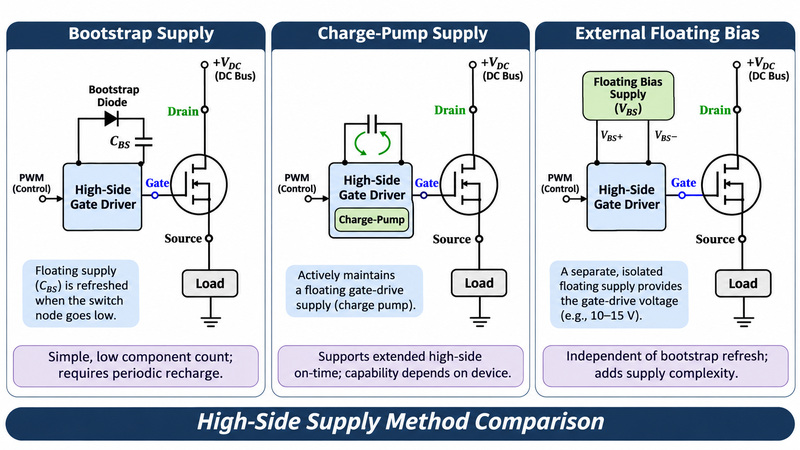
The supply method should be selected according to the actual switching pattern, not simply the nominal PWM frequency.
Check Duty Cycle and Bootstrap Refresh
Duty cycle becomes particularly important when the driver uses a bootstrap supply. Even if a bootstrap driver meets the voltage and current requirements, it may fail to maintain sufficient floating supply voltage during extended high-side conduction.
Maximum Duty Cycle and On-Time
For a periodic PWM control signal, duty cycle is:
Where tON is the high-side on-time and T is the switching period.
As duty cycle increases at a fixed PWM frequency, the available off-time decreases. This can reduce the time available to recharge the bootstrap capacitor. The critical parameter is not always duty cycle alone. The longest interval without effective bootstrap charging may occur during startup, pulse skipping, abnormal load conditions, or modulation patterns. Texas Instruments also discusses design considerations for 100% high-side duty-cycle operation using an additional floating supply [4].
A practical first estimate of the bootstrap capacitance is:
Where:
-
QG is the required gate charge.
-
QLS represents any applicable internal level-shifting charge.
-
IQBS is the floating driver's quiescent current.
-
ILEAK represents relevant leakage currents.
-
tHOLD is the maximum interval without recharge.
-
ΔVBS is the allowable bootstrap voltage drop.
This is a preliminary sizing relationship. The final capacitor must account for capacitance tolerance, DC-bias derating, temperature, and the selected driver's specific requirements. The allowable voltage drop must also leave sufficient margin above the driver's undervoltage threshold, and the minimum gate voltage required by the power device [3].
Bootstrap Recharge Conditions
A bootstrap capacitor can recharge only when the circuit provides a suitable charging path and sufficient voltage difference. In a conventional half-bridge, this commonly occurs when the low-side transistor conducts and pulls the switching node close to ground.
The required recharge interval depends on the bootstrap capacitance, diode characteristics, available supply voltage, and charging-path resistance. It is also important to check whether the bootstrap supply can be charged before the first high-side turn-on command [3].
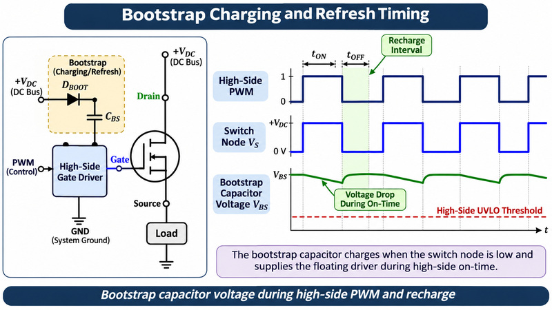
If the circuit cannot guarantee sufficient recharge time, consider a driver with verified charge-pump support or a separate floating bias supply.
Evaluate Drive Current and Timing
After confirming that the floating supply can operate reliably, evaluate whether the driver can switch the selected transistor at the required switching frequency and transition speed.
Source and Sink Current vs. Gate Charge
A gate driver must provide current to charge the transistor's gate during turn-on and remove that charge during turn-off. The required current depends on the device's gate charge and desired rise and fall time. A useful first-order relationship is:
Where IG is the approximate average gate current during the transition, QG is the relevant gate charge, and tSW is the targeted switching time. For example, transferring 100 nC of charge in 100 ns corresponds to an average current of approximately 1 A during that interval. However, the driver's advertised peak source and sink currents are not necessarily the currents available in the actual circuit.
The resulting gate current also depends on the driver's output resistance, external gate resistor, transistor characteristics, and circuit parasitics. A higher current rating and a suitable gate resistor can help control switching speed but faster is not always better. Excessive switching speed can increase ringing, electromagnetic interference, and voltage overshoot. Compare the driver's source and sink output current ratings separately, especially when fast turn-off is needed to reduce false turn-on risk [8].
Propagation Delay, Minimum Pulse Width, and Conditional Dead Time
Gate-driver timing affects the accuracy and safety of the switching sequence.
-
Propagation delay is the interval between an input command and the corresponding output response. Both turn-on and turn-off propagation delays should be examined. In a half-bridge, propagation delay mismatch can affect the effective dead time between the two switching devices.
-
Minimum pulse width determines how narrow an input pulse can be while still producing a valid output response. This becomes important as PWM frequency increases or the duty cycle approaches its limits.
-
Dead time is the intentional interval during which both half-bridge transistors are commanded off to prevent simultaneous conduction.
Some half-bridge drivers provide internal dead time control or interlock functions. Others require the PWM controller to manage timing externally.
These functions may depend on the input mode, channel configuration, or enable settings. Therefore, verify the driver's behavior for the actual control sequence rather than assuming that internal dead-time protection is always active. The final timing design must account for propagation delay tolerances, transistor switching characteristics, gate resistor value, and operating temperature.
Evaluate Transient Robustness and Isolation
High-side drivers experience switching-node voltage changes that can be much faster than the underlying PWM signal. A suitable driver must tolerate these transients without malfunctioning, exceeding its pin ratings, or unintentionally switching the power transistor.
Negative Switch-Node Transients
During switching, parasitic inductance and load current commutation can cause the switch node to fall below system ground. These negative voltage excursions may appear at the driver's high-side reference pin.
If the voltage exceeds the driver's permitted negative transient range, the result may be incorrect switching, supply disturbance, or device damage. Check the datasheet's negative switch-node transient specifications, including both the permitted magnitude and duration. Also examine the operating conditions under which those limits are specified. The driver's maximum high-side voltage rating does not establish its ability to tolerate negative transients. For example, the Infineon 2EDF5215G specifies device-specific negative high-side transient tolerance, illustrating why this parameter must be checked separately from the driver's nominal voltage rating [7, 11].
PCB layout also matters. Short gate-drive loops, appropriate decoupling, and careful management of high-current return paths help reduce unwanted switching-node disturbances.
High dV/dt, CMTI, and Miller-Induced False Turn-On
Fast-switching power devices can create large voltage slew rates at the switching node.
The slew rate is expressed as:
For an isolated or level-shifted driver, rapid common-mode voltage changes can disturb the transfer of control signals.
Common-mode transient immunity (CMTI) describes how well a driver maintains correct behavior during these changes. It is a particularly important specification for isolated drivers. The driver's stated CMTI should exceed the expected worst-case common-mode slew rate, with suitable margin and attention to test conditions [6].
Another concern is Miller-induced false turn-on. A rapid drain-to-source voltage change can couple current through the transistor's gate-drain capacitance:
This current can raise the gate voltage of a transistor that is supposed to remain off.
Possible countermeasures include stronger gate pull-down capability, an appropriately sized gate resistor, a negative off-state bias where appropriate, and an active Miller clamp.
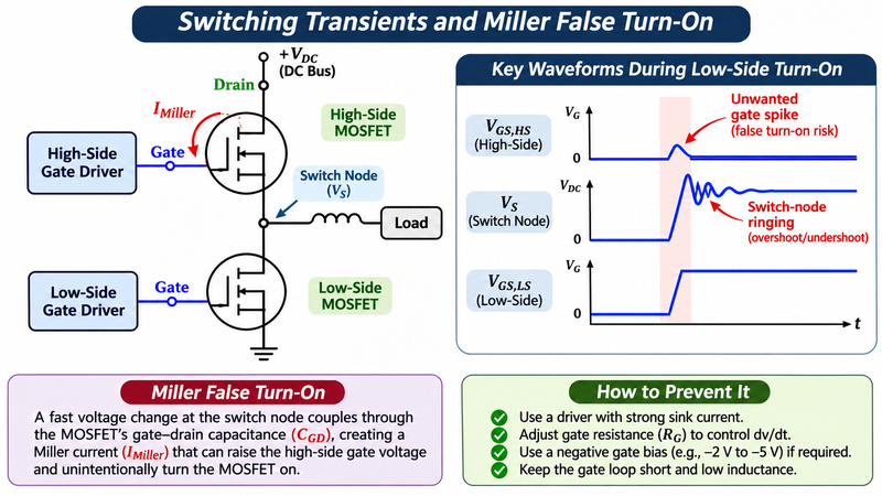
The correct choice depends on the power device's gate-voltage limits, switching speed, and the driver's available protection functions [8, 10].
When Galvanic Isolation Is Required
A floating high-side output and galvanic isolation are not the same thing. A non-isolated high-side driver may use level shifting and a floating supply while maintaining an electrical relationship with the controller-side circuitry.
Isolated gate drivers transfer control information across an insulation barrier, allowing the input and output sides to operate without a direct conductive signal path. Isolation may be necessary when the system requires electrical separation for safety, accommodates substantial differences between reference potentials, or must meet specific insulation requirements.
When selecting isolated gate drivers, examine their isolation class, working voltage, repetitive peak voltage, surge ratings, creepage, clearance, isolation capacitance, and CMTI. Do not rely solely on a headline isolation test-voltage rating. The driver's continuous operating capability and applicable safety standards must also be verified. Additionally, the isolated gate driver still requires a suitable output-side bias supply [2, 6].
Check Protection and Operating Requirements
Once the electrical and switching requirements are satisfied, review the driver's protection functions and operating limits. Protection features can reduce the risk of damage, but they must be compatible with the selected transistor and system-level fault strategy.
UVLO and Startup Behavior
Undervoltage lockout (UVLO) prevents or disables gate-drive operation when the relevant supply voltage falls below a specified threshold. High-side drivers may monitor the main supply, floating high-side supply, or both.
The UVLO thresholds must be compatible with the minimum voltage required to operate the external transistor safely. Check the rising and falling thresholds, hysteresis, output state during undervoltage, and recovery behavior.
Startup is especially important for bootstrap drivers because the floating supply may initially be uncharged. Verify what happens when power is first applied, when the controller is disabled, and when the supply recovers after an undervoltage event.
Shutdown, DESAT, Miller Clamp, Fault Reporting, and Interlock
Not every application needs every protection feature. The required functions depend on the power device, topology, and expected faults.
| Protection feature | Selection consideration |
|---|---|
| Shutdown or enable | Defined output behavior during disabled and fault conditions |
| DESAT detection | Short-circuit or abnormal conduction detection, especially relevant to IGBT and certain SiC MOSFET applications |
| Active Miller clamp | Helps keep the transistor off during high-voltage switching transients |
| Fault reporting | Provides status information to the controller |
| Interlock | Helps prevent simultaneous high-side and low-side conduction |
| Soft turn-off | Controls transistor turn-off during certain fault conditions to limit excessive stress |
For DESAT-based short circuit protection, review the detection threshold, blanking time, response delay, and fault-reset behavior. For an active Miller clamp, check when the clamp engages and whether its current capability is adequate for the expected transient [2, 10].
Fault reporting and shutdown behavior should also be evaluated together. A driver may detect a fault correctly but still require the external controller to perform part of the system recovery sequence. Protection functions should be verified against the complete fault response required by the design.
Package, Temperature, and Qualification
The final device must also meet the application's environmental and manufacturing requirements. Check the operating temperature range, thermal characteristics, package dimensions, and PCB layout requirements.
For high-speed designs, package parasitics and the availability of separate power and signal return connections may influence switching loss and overall performance.
Automotive applications may require AEC-Q100 qualification. Industrial or safety-related systems may have additional reliability and certification requirements.
Purchasing teams should also confirm the exact orderable part number, package option, availability, and manufacturer documentation before approving a component.
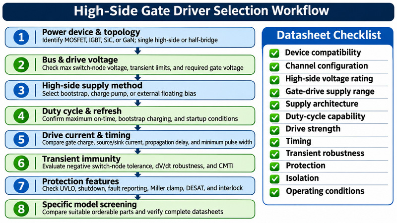
High-Side Gate Driver Selection Workflow
A structured selection process helps eliminate unsuitable parts early and prevents important specifications from being overlooked. Use the following decision sequence when comparing high-side gate-driver ICs.
Practical Selection Example: 400 V Half-Bridge with SiC MOSFETs
Consider a 400 V DC half-bridge using two Infineon IMW65R027M1H CoolSiC MOSFETs. Assume a switching frequency of 50 kHz and an application that may require extended high-side conduction. The objective is to identify a suitable gate driver using the electrical and operating requirements discussed above.
Step 1: Verify the Bus Voltage and Power Device
The IMW65R027M1H has a drain-source voltage rating of 650 V, providing a preliminary voltage-rating margin above the nominal 400 V DC bus [1]. However, the final selection must account for maximum bus voltage, switching overshoot, and voltage ringing to ensure that the MOSFET's limits are not exceeded.
Step 2: Determine the Required Gate-Drive Voltage
According to Table 4 of the Infineon datasheet [1], the recommended gate-source voltages are:
-
Turn-on voltage: +18 V
-
Turn-off voltage: 0 V
-
Gate-source operating range, including undershoot: −2 V to +20 V
Therefore, a gate driver capable of supplying an 18 V on-state gate voltage and a 0 V off-state voltage is appropriate for initial evaluation. Negative turn-off bias should not be assumed necessary for this device; the actual gate-voltage excursions must remain within the specified operating limits.
Step 3: Estimate the Required Gate-Drive Current
The MOSFET has a typical total gate charge of 62 nC, specified at VDD = 400 V, ID = 38.3 A, and VGS = 0 to 18 V [1].
A preliminary estimate of the average gate current during a transition is:
Assuming a target gate-charge transfer time of 100 ns:
This calculation gives an initial current estimate rather than a required peak-current rating.
One candidate is the Texas Instruments UCC21750, a single-channel isolated gate driver offering up to ±10 A peak source and sink current [2]. Its drive capability provides flexibility for selecting external gate resistance and adjusting switching speed.
The actual transition current and switching times must be checked against the driver's output resistance, MOSFET gate characteristics, gate resistors, and PCB parasitics.
Step 4: Evaluate Common-Mode Transient Immunity
Fast SiC switching produces rapid voltage changes between the high-side gate driver's input and output reference potentials. As an illustrative calculation, assume a 400 V switching-node transition occurs in 20 ns:
The UCC21750 specifies a minimum CMTI of 150 V/ns, providing substantial margin above this assumed switching slew rate [2, 6]. However, the actual worst-case common-mode slew rate, including ringing and both switching polarities, must be evaluated before confirming suitability.
Step 5: Select the High-Side Supply Method
A conventional bootstrap circuit could be considered if the half-bridge operates with regular switching intervals that allow the bootstrap capacitor to recharge [3]. However, if the high-side MOSFET must remain on continuously, a bootstrap-only arrangement cannot maintain its gate-drive supply indefinitely [4].
For this example, two UCC21750 single-channel isolated drivers can be evaluated, one for each MOSFET, with appropriate separately referenced output-side bias supplies. An 18 V gate-drive bias for each device would support the recommended +18 V/0 V switching levels without relying on bootstrap refresh.
At the assumed 50 kHz switching frequency, the approximate gate-charging power for each MOSFET is:
This is only the estimated gate-charging power. The final bias-supply design must also account for driver consumption, losses, decoupling, and operating margins.
Step 6: Check Protection and Timing
The UCC21750 includes DESAT-based fault detection, an active Miller clamp, undervoltage lockout, fault reporting, and soft turn-off [2]. These functions are useful in a fast-switching SiC half-bridge, where an unintended turn-on or short-circuit event can cause severe device stress.
Before final selection, the DESAT threshold and total fault-response time must be checked against the MOSFET's short-circuit behavior. Since two independent single-channel drivers are being considered, the PWM controller must also provide appropriate interlock and dead-time control, accounting for propagation-delay differences.
Selection Outcome
The UCC21750 is a reasonable preliminary candidate for the illustrated 400 V SiC half-bridge because its output supply range, peak drive capability, CMTI, and protection functions align with the initial requirements.
However, this is a preliminary selection rather than a verified circuit design. Final approval requires checking the complete datasheets, isolation requirements, maximum switching-node voltage, gate-voltage overshoot, thermal performance, PCB layout, and measured switching behavior.
Datasheet Parameter Checklist
Before finalizing a component, use the following checklist.
| Parameter | What to verify |
|---|---|
| Device compatibility | Supported MOSFET, IGBT, SiC MOSFET, or GaN type |
| Channel configuration | Single high-side, half-bridge, or independently controlled outputs |
| High-side voltage rating | Maximum operating switch-node voltage and transient limits |
| Gate-drive supply range | Required on/off gate voltages and driver supply limits |
| Supply architecture | Bootstrap, charge pump, or external floating bias support |
| Duty-cycle capability | Maximum high-side on-time and recharge requirements |
| Drive strength | Source/sink current, output resistance, and gate-charge suitability |
| Timing | Propagation delay, matching, pulse width, and dead-time behavior |
| Transient robustness | Negative switch-node tolerance, slew-rate immunity, and CMTI |
| Protection | UVLO, shutdown, DESAT, Miller clamp, and interlock |
| Isolation | Required isolation type, working voltage, and insulation ratings |
| Operating conditions | Temperature, package, thermal performance, and qualification |
Frequently Asked Questions
Can a bootstrap high-side gate driver operate at 100% duty cycle?
A conventional bootstrap-only supply cannot maintain the high-side transistor on indefinitely without recharging. Some drivers support 100% duty cycle through an integrated charge pump or another supply arrangement. Always check the specific device specification [4, 5].
Is a high-side driver's voltage rating the same as its gate-drive voltage?
No. The high-side voltage rating relates to the switching-node voltage the driver can tolerate. The gate-drive voltage determines the voltage applied between the power transistor's gate and source or emitter.
Do all high-side gate drivers require isolation?
No. Many high-side drivers use non-isolated level shifting and floating supplies. Galvanic isolation is required only when the system's electrical separation, safety, or functional requirements call for it.
Can the same driver be used for silicon MOSFETs and GaN devices?
Only if the driver's voltage range, timing, output characteristics, and transient performance meet the requirements of the specific devices. GaN devices often require more tightly controlled gate voltages.
Is higher gate-driver current always better?
Not necessarily. Higher drive current can reduce switching time, but excessive switching speed may increase ringing and EMI. The drive strength should be selected according to gate charge, desired switching behavior, and circuit layout.
What should be checked first when comparing high-side drivers?
Begin with the power device and topology, followed by the maximum bus voltage, required gate-drive voltage, and high-side supply method. These factors usually eliminate unsuitable drivers before detailed timing and protection comparisons.
Conclusion
Selecting a high-side gate driver involves several related decisions. The driver must support the chosen power transistor, withstand the application's operating voltage and transients, and maintain an appropriate floating supply throughout the switching cycle.
Duty-cycle requirements are especially important when choosing between bootstrap, charge-pump, and external floating-bias solutions. Drive current, timing, transient immunity, and protection features then determine whether the driver can operate reliably in the intended circuit.
A practical approach is to establish these requirements first, shortlist suitable models through Unikeyic's Gate Drivers category, and verify every critical parameter against the manufacturer's datasheet before making the final selection.
References
The following manufacturer datasheets, application notes, and technical resources provide supporting information for the gate-driver selection criteria and practical example discussed in this guide.
-
Infineon Technologies. IMW65R027M1H CoolSiC MOSFET 650 V G1 Datasheet, Revision 2.3, January 2025. Device voltage ratings, gate-drive voltage, gate charge, and electrical characteristics. Infineon IMW65R027M1H Datasheet
-
Texas Instruments. UCC21750: 10-A Source/Sink Reinforced Isolated Single-Channel Gate Driver for SiC/IGBT, Datasheet. Covers drive current, CMTI, isolation ratings, DESAT, active Miller clamp, and soft turn-off. TI UCC21750 Product and Datasheet
-
Texas Instruments. Bootstrap Circuitry Selection for Half-Bridge Configurations, Application Note SLUA887A, revised September 2023. Covers bootstrap capacitor sizing, gate charge, driver current consumption, recharge conditions, and component selection. TI SLUA887A: Bootstrap Circuitry Selection
-
Texas Instruments. Using Half-Bridge Gate Driver to Achieve 100% Duty Cycle for High Side FET, Application Note SLUAAV9, March 2024. Explains the limitations of bootstrap-only circuits and the use of an additional floating supply. TI SLUAAV9: 100% High-Side Duty Cycle
-
Analog Devices. LTC7001: Fast 150 V High-Side NMOS Static Switch Driver, Product Datasheet. Demonstrates an integrated charge-pump solution supporting 100% duty-cycle operation in its specified lower-voltage range. Analog Devices LTC7001 Product and Datasheet
-
Texas Instruments. Application Brief SLUAAZ0A, September 2025. Discusses common-mode transient immunity, isolated gate-driver behavior, testing conditions, and isolation considerations. TI SLUAAZ0A: Common-Mode Transient Immunity
-
Texas Instruments. How to Achieve Higher System Robustness in DC Drives, Part 1: Negative Voltage, Technical Article SSZT741, April 2018. Explains negative switching-node transients and their effects on high-side gate drivers. TI SSZT741: Negative Voltage in DC Drives
-
Infineon Technologies. Gate Driver Requirements for MOSFETs, IGBTs, SiC and GaN. Technical guidance covering technology-specific gate voltages, switching behavior, UVLO, isolation, and protection requirements. Infineon Gate Driver Requirements Guide
-
Texas Instruments. GaN Parameter Advantages, Application Brief SLUAAM0, August 2022. Discusses GaN gate-voltage limitations, switching requirements, and dedicated GaN gate-driver considerations. TI SLUAAM0: GaN Parameter Advantages
-
Infineon Technologies. EiceDRIVER 1ED Family: Technical Description, Application Note. Explains IGBT drive behavior, desaturation detection, blanking-time design, fault handling, and active Miller clamping. Infineon EiceDRIVER 1ED Family Application Note
-
Infineon Technologies. EiceDRIVER 2EDF5215F, 2EDF5215G Datasheet. Covers high-side and low-side voltage ratings, negative HS transient immunity, and switching specifications. Infineon 2EDF5215F / 2EDF5215G Datasheet