Effect of Miller Capacitance:An Invisible Challenge in High-Frequency Circuit Design
In electronic circuit design, high-frequency response characteristics often set the upper limit of an electronic system's performance. When engineers attempt to enhance amplifier bandwidth or optimize RF circuits, a phenomenon known as the "Effect of Miller Capacitance" frequently emerges as a critical bottleneck, hauntingly reminiscent of an elusive specter. Proposed by American engineer John Milton Miller in 1920, this effect reveals how hidden capacitive coupling mechanisms within circuits can dramatically constrain high-frequency digital signals through constant voltage feedback. This article delves into the classic electronics phenomenon across four dimensions: physical mechanism, mathematical modeling, engineering impact, and strategies for mitigation.
I. Physical Mechanism: The "Mirrored Amplification" of Bridging Capacitance
At the heart of the Miller capacitance effect lies the parasitic capacitance bridging the input and output nodes of a circuit. Taking a typical common-emitter transistor amplifier as an example, the junction capacitance C(bc) naturally exists between the transistor base (B) and collector terminals(C), forming a capacitive path from the input to the output when the circuit is operational.
When the amplifier operates in an inverting amplification mode (voltage gain (Av=Vout/Vin<0), the output impedance exhibits a 180° phase difference relative to the input signal. Consequently, the voltage amplifier across the bridging capacitance C(bc) is:

Applying the larger capacitor energy formula, the equivalent charge variation observed at the input equates to a virtual stray capacitance:
Given that A(v) is negative, the effective capacitance is amplified as (C(bc) ⋅(1+∣A(v)∣). For instance, with a voltage gain of -100, a actual capacitance of 5pF translates to an equivalent input capacitance of 505pF—this "capacitance multiplication" directly alters the frequency response characteristics of the circuit.
II. Mathematical Modeling: The Dimensionality Reduction of Miller's Theorem
To accurately quantify the influence of the Miller effect, engineers commonly utilize Miller's Theorem for circuit analysis. This theorem simplifies the cross-coupling stray capacitance into two separate capacitors at the input/output terminals:
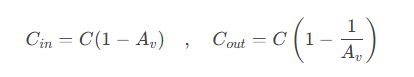
This transformation streamlines the complex dual-node coupling issue into a single-node analysis. In a common-emitter amplifier, the input-side equivalent capacitance C(in), along with the base resistance R(π), forms a low-pass filter, whose cutoff frequency is:
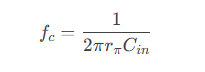
Assuming ( R(π)=1kΩ,C(in)=505pF ), the cutoff frequency drops to 315kHz—a bandwidth limitation disastrous for RF circuits requiring MHz-level signal conditioning.
III. Engineering Impact: Design Dilemmas from Amplifiers to Chip Level
Bandwidth Collapse
The input capacitance multiplication induced by the Miller effect leads to a sharp decline in the high-frequency gain of amplifiers. In operational amplifiers, this manifests as a -20dB/decade roll-off in the open-loop gain curve, making the gain-bandwidth product (GBW) a crucial performance metric.
Phase Crisis
Additional phase shifts introduced by the equivalent additional capacitance can destabilize feedback digital systems. In a typical collector voltage follower circuit, if the Miller effect causes total phase shift to reach 180°, negative feedback turns into positive feedback, driving the circuit into self-oscillation.
Cascading Disasters
In multi-stage amplifier circuit performance, cumulative Miller capacitance effects can drastically reduce total bandwidth—potentially reducing the overall bandwidth of a three-stage amplifier to just one-third that of a single stage. This poses significant challenges for applications like high-speed ADC driver circuits.
IV. Strategies for Overcoming Miller's Shackles: An Engineer's Toolbox
Faced with the constraints of the Miller effect, electronic engineers have developed a multi-layered strategy:
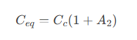
Miller Compensation Techniques
In operational amplifier design, engineers cleverly use the Miller effect for phase compensation. By introducing a compensation capacitor C(c) between the output stage and input stages, its equivalent input capacitance becomes:

where A(2) is the second-stage gain. This active compensation pushes the dominant pole to lower frequencies, forcing the gain curve to cross the 0dB line at a -20dB/decade slope, ensuring a phase margin >45°. This common technique is exemplified in the internal structure of μA741 op amps.
Cascode Structure Revolution
Cascading a common-emitter amplifier with a common-base amplifier effectively isolates the C(bc) feedback path through the low input impedance characteristic of the common-base stage (Figure 2). Experiments show that the Cascode structure can increase high-frequency cutoff frequency more than tenfold, becoming a standard configuration in high-speed amplifiers.
Neutralization Circuit Magic In rf amplifier detailed design, engineers introduce a neutralization capacitor C(n) (Figure 3), generating opposing feedback current flowing to those of C(bc). When:
the two currents cancel each other, perfectly eliminating the Miller effect. This technique enabled vacuum tube radios in the 1940s to achieve stable MHz-level amplification.
Process-Level Breakthroughs
Modern semiconductor processes reduce parasitic capacitance by optimizing transistor structures. For example, SiGe HBT transistors feature C(bc) values an order of magnitude lower than traditional BJTs, while GaN devices compress parasitic capacitance to the femtofarad frequency range with their two-dimensional electron gas structures.
V. The Future Battlefield: New Challenges at the Nanoscale
In the era of 5G millimeter-wave and optical communications, electronic circuit operating frequencies have surpassed the 100GHz threshold. Traditional Miller effect models now require distributed parameter corrections:
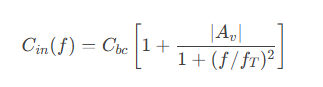
where f(T) is the transistor cutoff frequency. As the operating frequency approaches f(T), the magnification factor of the Miller capacitance begins to diminish, offering new optimization opportunities for ultra-high-frequency circuit design.
Emerging semiconductor technologies such as quantum dot transistors and carbon nanotube active devices are fundamentally reconstructing the physical mechanisms of parasitic capacitance. In 2021, IBM's development of a 2nm chip using nanosheet structures reduced gate capacitance by 45%, heralding new pathways to combat the Miller effect in the post-Moore era.
An Eternal Struggle From vacuum tubes to FinFETs, from kHz to THz, the Miller capacitance effect has persistently accompanied the evolution of electronic technology. This ongoing battle between engineers and the laws of physics not only demonstrates the unforgiving nature of natural laws but also highlights the brilliance of human ingenuity. As we integrate billions of transistors onto a chip, each successful timing convergence, every increment in bandwidth, narrates the epic struggle against the Miller effect. This may well be the charm of electronic engineering—innovation within constraints, triumph over limitations.