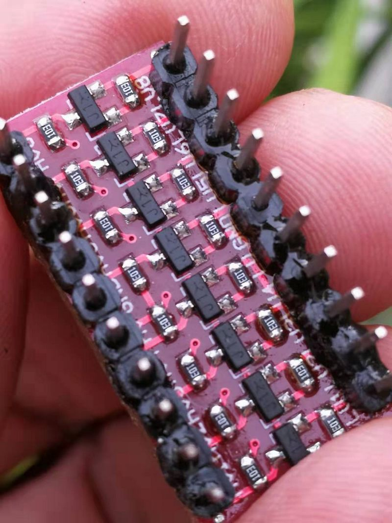
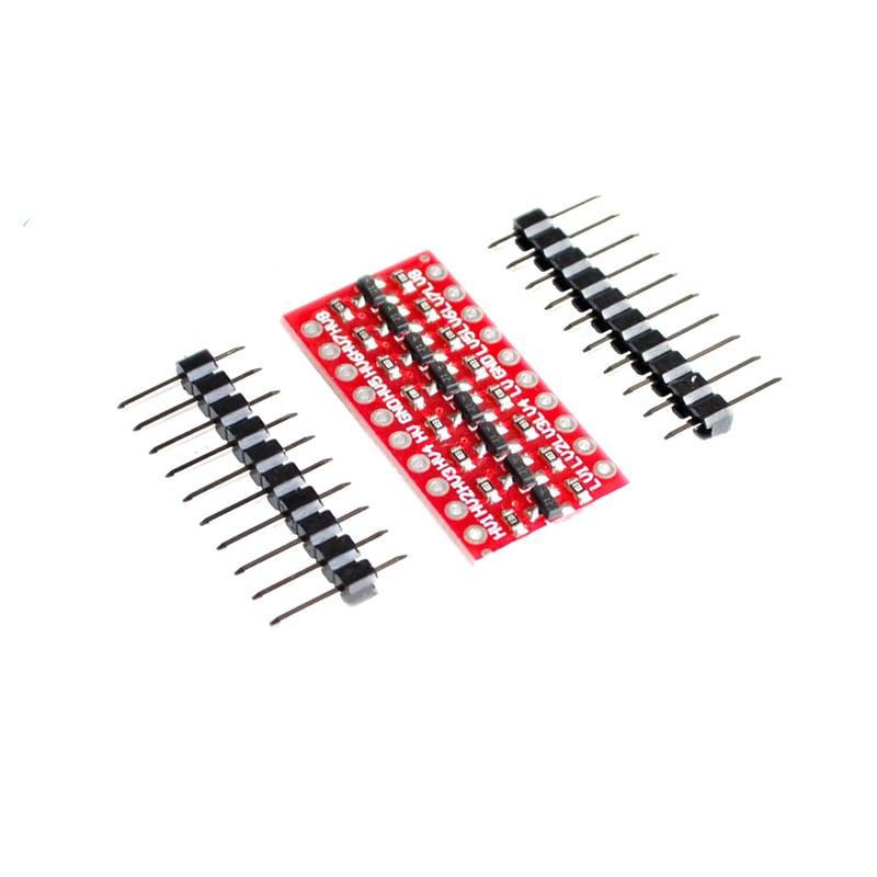
Arduino Hands-on- 8-bit Bidirectional Voltage Level Conversion Module
Experiment: 8-bit 5V-3V IIC UART SPI TTL bidirectional level conversion module.
A voltage level converter, also known as a level shifter, is an electronic device used to convert the voltage level of a signal. Voltage level conversion can be categorized into unidirectional and bidirectional conversion, as well as single-supply and dual-supply conversion. Dual-supply conversion employs a dual-rail scheme to meet various performance requirements. In the design of new-generation electronic circuits, the introduction of low-voltage logic often leads to issues of mismatched input/output logic within systems, thereby increasing the complexity of system design. For example, when a 1.8V digital circuit needs to communicate with a 3.3V analog circuit, the conversion between the two voltage levels needs to be addressed first, necessitating the use of a voltage level converter.
With the emergence of digital ICs operating at different supply voltages, the necessity of logic level conversion becomes more prominent. The methods of level shifting will also vary depending on the logic voltage, data bus format (such as 4-wire SPI, 32-bit parallel data bus, etc.), and different data transfer rates. While many logic chips can now achieve high-to-low logic level conversion (such as converting from 5V to 3V), very few can perform low-to-high logic level conversion (such as converting from 3V logic to 5V logic). Furthermore, although voltage level converters can be implemented using transistors or even resistor-diode combinations, these methods are greatly limited by parasitic capacitance, which significantly restricts data transfer rates.
Despite commercially available wide-byte level converters, these products are not optimized for serial buses with data rates below 20Mbps (such as SPI™, I2C™, USB, etc.). These devices typically have larger package sizes, more pins, and I/O direction control pins, making them unsuitable for small-scale serial or peripheral interfaces and higher-speed buses (such as Ethernet, LVDS, SCSI, etc.).
Logic Voltage Levels
The so-called voltage level refers to the logarithm of the ratio between two power levels or voltages, and sometimes it can also be used to indicate the logarithm of the ratio between two current levels. The unit for voltage level is decibels (dB). Commonly used voltage levels include power voltage level and voltage voltage level, each of which can further be divided into absolute voltage level and relative voltage level. Logic voltage level refers to a state that can generate signals, usually manifested by the potential difference between the signal and the ground wire. The fluctuation range of logic voltage level is determined by the characteristics of different devices in the logic family.
Regarding logic high and low voltage levels:
•l In 5V CMOS, HC, AHC, and AC, input greater than 3.5V is considered as high voltage || input less than 1.5V is considered as low voltage;
•l In 5V TTL, ABT, AHCT, HCT, and ACT, input greater than 2V is considered as high voltage || input less than 0.8V is considered as low voltage;
•l In 3.3V LVTTL, LVT, LVC, ALVC, LV, and ALVT, input greater than 2V is considered as high voltage || input less than 0.8V is considered as low voltage;
•l In 2.5V CMOS, ALVC, LV, and ALVT, input greater than 1.7V is considered as high voltage || input less than 0.7V is considered as low voltage.
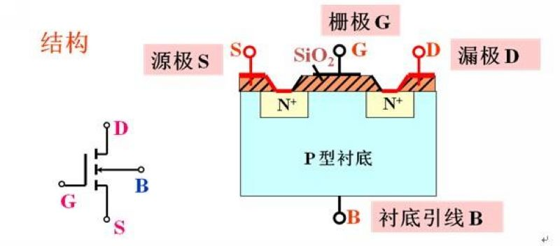
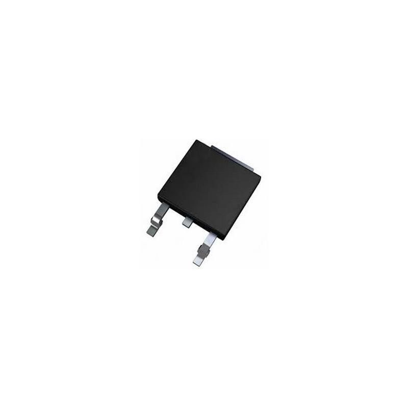
Field Effect Transistor (FET), also known as field-effect transistor, is mainly divided into two types: junction FET (jfet) and metal-oxide semiconductor FET (MOS-FET). It relies on majority carriers for conduction, hence also referred to as unipolar transistor. Belonging to the
category of voltage-controlled semiconductor devices, FET boasts high input resistance (107~1015Ω), low noise, low power consumption, wide dynamic range, easy integration, absence of secondary breakdown phenomenon, and a broad safe operating area. Consequently, it has emerged as a strong competitor to bipolar transistors and power transistors. FET is a type of semiconductor device that utilizes the electric field effect of the control input circuit to regulate the current flow in the output circuit, and is named accordingly. Given that it conducts electricity solely through majority carriers within the semiconductor, it is also known as unipolar transistor.
Field-effect transistors, also known as FETs, are used for various purposes.
The working principle of a field-effect transistor can be summarized as follows:"The current flowing from the drain terminal to the source terminal through the channel, known as ID, is controlled by the reverse-biased gate-to-channel pn junction voltage." More accurately, the width of the channel, which is the cross-sectional area through which ID flows, is influenced by changes in the depletion layer caused by the reverse biasing of the pn junction. In the non-saturation region when VGS=0, the expansion of the depletion layer is limited. Due to the electric field generated by the VDS applied between the drain and source terminals, some electrons from the source region are pulled towards the drain, resulting in a current flow (ID) from drain to source. The depletion layer expanding from the gate towards the drain partially blocks the channel, leading to ID saturation. This state is referred to as pinch-off, where the depletion layer restricts a portion of the channel but does not completely cut off the current flow. In the ideal scenario, the depletion layer has insulating properties due to the absence of free electrons or holes, making current flow difficult. However, the strong electric field between the drain and source terminals allows high-speed electrons to pass through the depletion layer, causing ID saturation. Furthermore, when VGS becomes negative and reaches VGS(off), the depletion layer covers the entire channel area. Most of the electric field from VDS is concentrated on the depletion layer, directing electrons towards the drift direction, except for a very short section near the source terminal which further inhibits current flow.
Applications:
•l Field-effect transistors can be used for amplification.
•l Their high input impedance makes them suitable for impedance transformation.
•l They can be utilized as variable resistors.
•l Field-effect transistors are convenient for use as current sources.
•l They can serve as electronic switches.
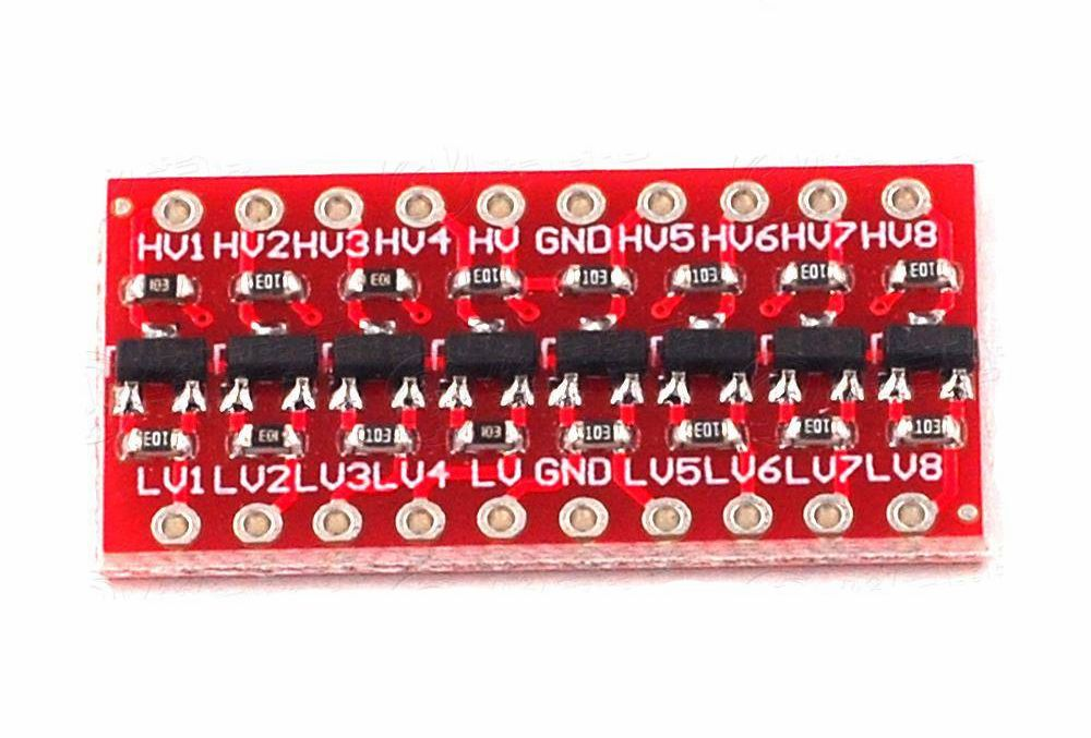
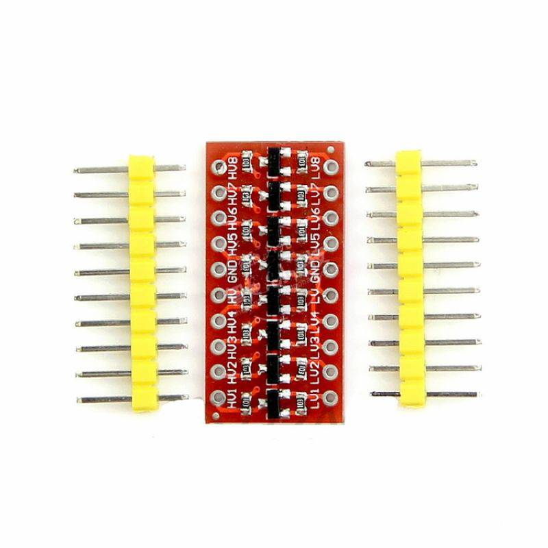
Eight MOS tubes are used to achieve a bidirectional level conversion module for eight channels of 3V and 5V voltage levels.
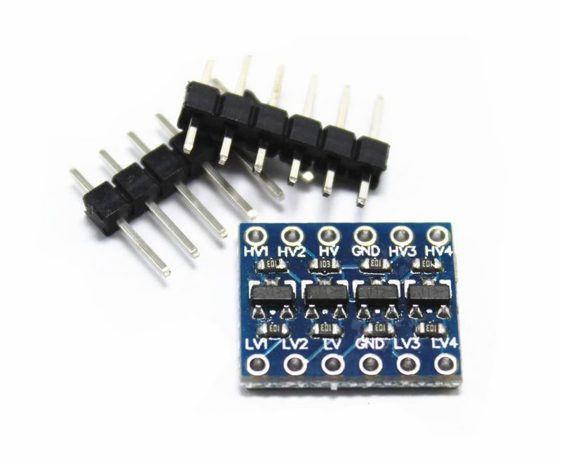
If you have ever attempted to connect a 3.3V device to a 5V system, you know the challenge it poses. A bidirectional logic level converter is a small device that can safely lower 5V signals to 3.3V and boost 3.3V to 5V. This level shifter is also compatible with 2.8V and 1.8V devices. The key difference of this logic level converter from its predecessors is the ability to confidently set high and low voltages and safely shift them on the same channel. Each level shifter has the capability to convert 4 pins on the high side to 4 pins on the low side, providing two inputs and two outputs for each side.
The level converter is very easy to use. The circuit board needs to be powered by two voltage sources used by the system (high voltage and low voltage). Connect the high voltage (e.g. 5V) to the "HV" pin, the low voltage (e.g. 3.3V) to the "LV" pin, and ground from the system to the "GND" pin.
Compatible with 5-3V systems
Connect VIN to the 5V system power supply
Connect 5A to the 5V system
Connect 5B to the 5V system
Connect GND to the GND of the 5V system
Connect 3V3 to the 3V system power supply
Connect 3A to the 3V system
Connect 3B to the 3V system
Connect GND to the GND of the 3V system
Dimensions: 28×19mm / 1.1×0.74 inches
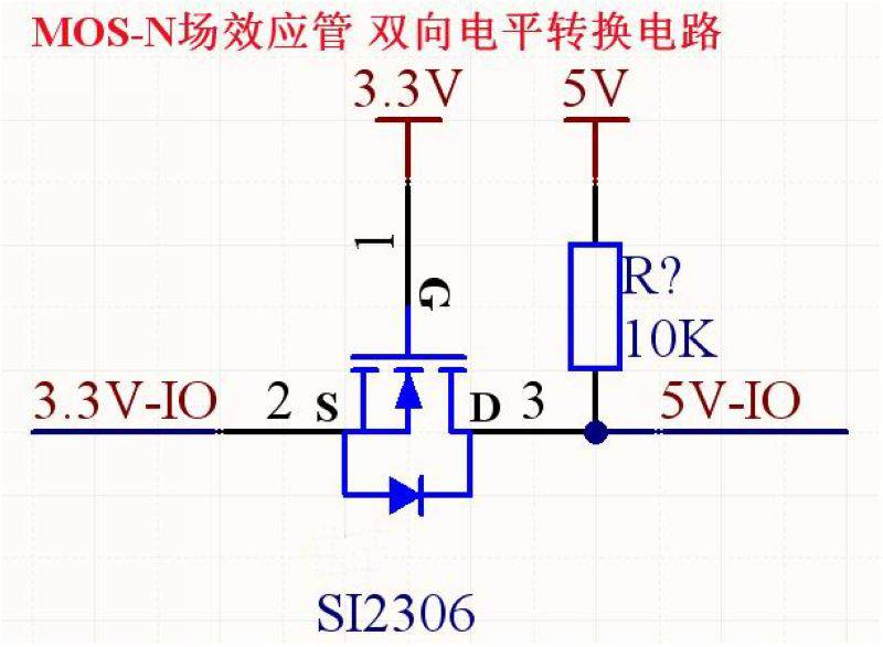
Principle of Bidirectional Transmission:
For the sake of simplicity, let's define 3.3V as end A and 5.0V as end B.
When end A outputs a low level (0V), the MOS tube conducts, resulting in a low-level output (0V) at end B.
When end A outputs a high level (3.3V), the MOS tube cuts off, leading to a high-level output (5V) at end B.
When end A is in a high-impedance state (OC), the MOS tube cuts off, resulting in a high-level output (5V) at end B.
When end B outputs a low level (0V), the diode inside the MOS tube conducts, causing the MOS tube to conduct, resulting in a low-level output (0V) at end A.
When end B outputs a high level (5V), the MOS tube cuts off, leading to a high-level output (3.3V) at end A.
When end B is in a high-impedance state (OC), the MOS tube cuts off, resulting in a high-level output (3.3V) at end A.
Advantages:
•l Suitable for low-frequency signal level conversion at a low cost.
•l The voltage drop after conduction is smaller compared to a transistor.
•l Bidirectional conduction, akin to a mechanical switch.
•l Voltage-driven, requiring a certain amount of driving current, which may be larger than that of a transistor in some applications.
Module Features:
The eight MOS tube level module achieves bidirectional conversion between 3V and 5V levels for eight channels.
Power input with reverse connection protection, integrated 3.3V LDO, and capable of providing an external current not exceeding 150mA.
Equipped with a power indicator light for clear indication of operation status.
Can achieve bidirectional conversion of bus signals such as UART, IIC, 1-wire, and SPI between 3V and 5V levels.
Eight-channel high-voltage logic and low-voltage logic bidirectional conversion, enabling bidirectional conversion between HV and LV.
LV connects to 3.3V power supply
HV connects to 5V power supply
GND connects to the negative pole of the power supply, with both power supplies sharing a common ground
LV1-4 inputs 3.3V TTL level, HV1-4 outputs 5V TTL level
HV1-4 inputs 5V TTL level, LV1-4 outputs 3.3V TTL level
Schematic diagram of connecting Arduino to module using logic level converter
In this simple diagram, the Arduino Uno is connected to the ESP8266 WIFI module. When unsure of the voltage levels supported by the input/output pins of the module used, employing a logic level converter may be a relatively safe choice. In the diagram below, instead of directly connecting the TX and RX lines of the ESP8266 to the GPIO pins of the Arduino, they are connected to a logic level converter: connecting ESP8266 to Arduino Uno via a logic level converter is a wise approach. The logic level converter is a small yet very useful device. It helps in connecting devices with logic signals that operate at different voltage levels.

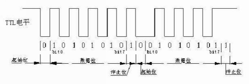
Results of the experiment regarding the serial port

Experimental scene diagram