MLX90614 Human Body Infrared Thermometer Gun based on STM32
Here, I will write about the driver code for the MLX90614 infrared temperature sensor and explain its principle. The main idea is to utilize the STM32F103C8T6 microcontroller and the MLX90614 module to display the measured temperature on a 0.96-inch OLED screen. If you don't have an OLED screen, you can also use a serial debugging assistant to print out the temperature information.
1.Materials Required
STM32F103C8T6 minimum system board + MLX90614 infrared temperature sensor module + 0.96-inch OLED display + a J-Link downloader.
2.Introduction to the MLX90614 Sensor
The MLX90614 series module is a universal infrared temperature sensor module. Before leaving the factory, this module has been calibrated and linearized, boasting advantages such as non-contact measurement, small size, high accuracy, and low cost. It provides two output interfaces for the measured target temperature and ambient temperature, making it suitable for applications in automotive air conditioning, indoor heating, household appliances, handheld devices, and medical equipment. Temperature measurement can be categorized into contact and non-contact methods. Contact temperature measurement can only measure the temperature of the object when it reaches thermal equilibrium with the sensor, resulting in longer response times and susceptibility to environmental temperature influences. In contrast, infrared temperature measurement uses the infrared radiation energy of the object to determine its temperature without physical contact. This method does not disturb the temperature distribution field of the object, offers high temperature resolution, fast response times, wide temperature measurement range, no upper limit on measurement temperature, and good stability, making the MLX90614 an ideal choice for our infrared temperature module.
The communication protocol between the microcontroller and the MLX90614 infrared temperature sensor is similar to I2C communication but is not exactly the same; it is known as "SMBus." SMBus (System Management Bus) is an efficient synchronous serial bus proposed by Intel in 1995, featuring only two signal lines: a bidirectional data line and a clock signal line. SMBus allows CPUs to communicate and exchange information with various peripheral interface devices in a serial manner, enhancing transmission speed and reducing device resource usage. Even in microcontrollers without an SMBus interface, software can simulate this communication protocol.
3.Working Principle of MLX90614
The MLX90614 consists of an MLX81101 infrared thermopile sensor and an MLX90302 signal processing chip, which includes a voltage regulator circuit, low-noise amplifier, A/D converter, DSP unit, pulse width modulation circuit, and logic control circuit.
Its working principle involves the temperature signal output by the infrared thermopile sensor being amplified by an internal low-noise, low-offset operational amplifier (OPA) and then converted into a 17-bit digital signal through an A/D converter (ADC). This signal is processed by a programmable FIR and IIR low-pass digital filter (DSP) before being output. The output results are stored in its internal RAM storage unit.
The MLX90614 contains two types of memory: EEPROM and RAM.
There are a total of 32 16-bit word EEPROM storage units in the MLX90614, with addresses ranging from 000H to 01FH.
All registers in the EEPROM can be read via SMBus, but only certain registers can be modified (addresses 0x00, 0x01, 0x02, 0x03, 0x04, 0x05*, 0x0E, 0x0F, 0x09).
Tomax and Tomin are the set upper and lower limits for measuring object temperature, while Ta represents the ambient temperature range.
The calculation method for the upper limit of the measured temperature is: Tomax = 100 × (To MAX + 273.15). The calculated result is then written to address 000H. The calculation method for the lower limit of temperature is the same as the upper limit calculation method, with the result being written to address 001H.
In the MLX90614, there are a total of 32 17-bit RAM storage units. Users cannot write data to RAM directly; they can only read 16-bit stored data from certain RAM storage units. The collected ambient temperature data is saved in storage unit address 006H, while the measured object temperature data is stored in storage unit address 007H. By utilizing the data stored in RAM addresses and following the calculation formula, the ambient temperature Ta and the object temperature To can be obtained.
Ta and To can be read and output via SMBus from the RAM units with a resolution of 0.02°C (fixed range), or they can be output in PWM digital mode with 10-bit resolution and configurable range. Since the temperature range of the measured temperature matches the temperature range calibrated by the MLX90614 during production, temperature data for Ta and To can be directly accessed and read via SMBus.
Ta = RAM(006H) x 0.02 - 273.15
To = RAM(007H) x 0.02 - 273.15
4.Principle of IIC Protocol
The communication steps between IIC master and slave are as follows:
The master sends a start signal to notify all slaves to be ready.
The master sends the slave address along with the read/write flag (0 for write, 1 for read). The slave address and read/write flag together occupy 8 bits, with the address using the high 7 bits and the read/write flag using the lowest bit.
The slave responds to the master (ACK).
In write mode, after receiving the ACK, the master sends one byte of data and waits for the slave's response. If there is more data to send, the master continues sending subsequent data segments until the transmission is complete. In read mode, the STM32 master reads the data sent by the slave, responds to the slave, and if the slave has more data to send (continuing to report the second segment), the master continues reading, sending a response back to the slave.
The master sends a stop signal to the slave.
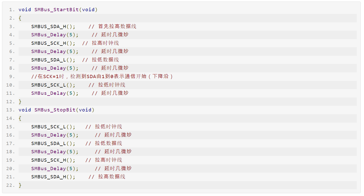
4.1 Write Timing Sequence
First, the master device sends a start bit, followed by sending the slave address 0x00 and the write flag 0, totaling 8 bits. After transmitting these 8 bits, the master device waits for the slave's response. If the slave sends an acknowledgment signal, the master continues to send one byte of data to the slave. The process repeats, waiting for the slave's response each time. The master continues sending subsequent data segments until the transmission is complete.
Functions used in the write sequence include:
void SMBus_StartBit(void); — Master device sends a start bit.
u8 SMBus_SendByte(u8 ack_nack); — Master device sends the slave's address and write flag.
SMBus_ReceiveBit(ack_nack); — Slave device sends an acknowledgment signal.
u8 SMBus_SendByte(u8 ack_nack); — Master device sends one byte of data to the slave.
void SMBus_StopBit(void); — Master device sends a stop bit.
4.2 Read Timing Sequence
In the read timing sequence:
The master device initiates by sending a start bit, followed by transmitting the slave address 0x00 and the read flag 1, totaling 8 bits. After sending these 8 bits, the master device awaits the response from the slave. If the slave responds with an acknowledgment signal, the slave sends one byte of data to the master.
During reading, the master reads data from the slave, while conversely, the slave sends data to the master. Similarly, after sending one byte of data, the slave also needs to inquire whether to continue sending to the master. If the master signals to continue (by sending an acknowledgment signal), the slave continues sending data. This process repeats after each data transmission until the master signals a non-acknowledgment, at which point the slave stops sending data. Finally, the master sends a stop signal.
Functions used in the read sequence include:
void SMBus_StartBit(void); — Master device sends a start bit.
u8 SMBus_SendByte(u8 ack_nack); — Master device sends the slave's address and read flag.
SMBus_ReceiveBit(ack_nack); — Slave sends an acknowledgment signal.
u8 SMBus_ReceiveByte(u8 ack_nack); — Slave sends one byte of data to the master.
void SMBus_StopBit(void); — Master sends a stop bit.
4.3 Communication Process
Start Signal - The start signal is generated when the data line SDA transitions from high to low during a high clock signal period on the SCL line.Acknowledgment Signal - During a high clock signal period on the SCL line, the data line SDA remains low to indicate an acknowledgment signal.Non-Acknowledgment Signal - During a high clock signal period on the SCL line, the data line SDA remains high to indicate a non-acknowledgment signal.Stop Signal - The stop signal is generated when the data line SDA transitions from low to high during a high clock signal period on the SCL line.Data Signal - During data transmission, when the clock line SCL is high, if the data line SDA is high, it represents binary 1. Similarly, when the clock line SCL is high, if the data line SDA is low, it represents binary 0.
The first box represents the SDA data valid period, and the second box represents the data change period.
5.Program Coding
5.1 Start Signal and Stop Signal
5.2 Transmitting a Byte
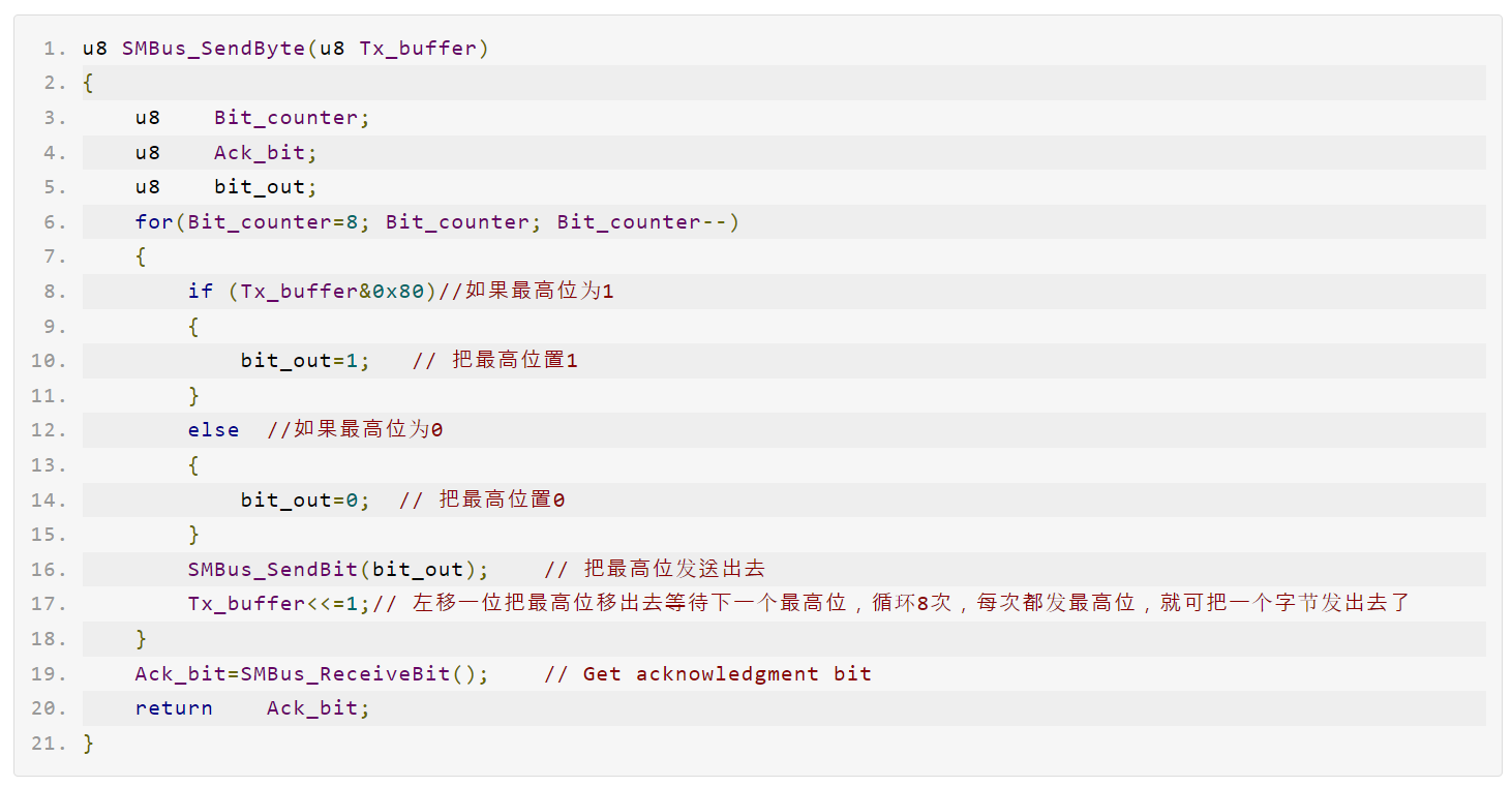
To transmit a byte, which consists of 8 bits, we iterate through each bit and send the most significant bit first. If the most significant bit is 1, we perform a bitwise "AND" operation between the byte Tx_buffer and 0x80 (10000000) to set the most significant bit to 1. If the most significant bit is 0, we ensure it remains 0. Then, we use SMBus_SendBit(bit_out); to send out the most significant bit. Afterwards, we shift Tx_buffer left by one bit with Tx_buffer <<= 1; to prepare for sending the next highest bit. This process repeats 8 times to send out all 8 bits of the byte.
When sending a byte via SMBus, after the slave sends one byte, the master needs to respond with an acknowledgment signal to indicate whether to continue sending the next byte. Therefore, we use the statement Ack_bit = SMBus_ReceiveBit(); to determine if the slave should continue sending the next byte. If the returned value is 0, the transmission continues; if it is 1, the transmission stops.
5.3 Receiving a Byte
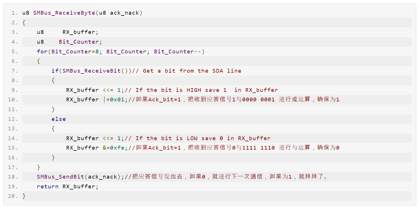
When receiving a byte from the SMBus, which consists of 8 bits, we also use a for loop to receive each bit one by one. Initially, we use an if statement to check if SMBus_ReceiveBit() has received an acknowledgment signal. If an acknowledgment signal is received (denoted by 1), we shift the received data left by one bit with RX_buffer <<= 1;. If the bit shifted out becomes 1, we perform a bitwise "OR" operation with 0x01 (0000 0001) to ensure it is set to 1. If the shifted bit is 0, we perform a bitwise "OR" operation with 0xfe (1111 1110) to ensure it remains 0. Finally, we send out the acknowledgment signal via SMBus. If the received signal is 0, the communication continues; if it's 1, the process ends and no further data is accepted.
5.4 Data Verification
Data verification is crucial to ensure the accuracy of the collected data.
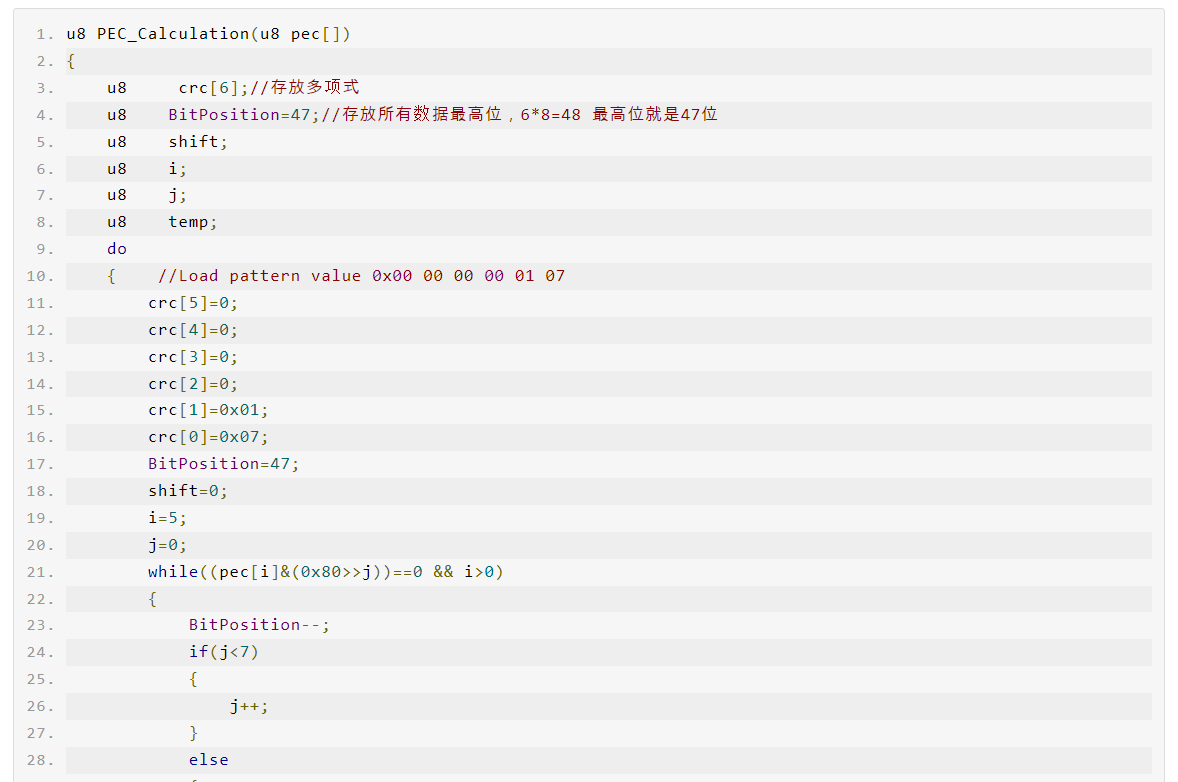
In our program, the PEC data is read out through SA_W, Command, SA_R, LSByte, and MSByte. Subsequently, we need to create a verification function to determine whether the received PEC data is correct. Only when the data verification passes can we proceed to the next evaluation step. If the verification fails, we continue reading until the correct data is obtained. How can we confirm if the data we have read is correct? To do this, you need to create a separate C project and run the function u8 PEC_Calculation(u8 pec[]) within it. By inputting data such as 0x00, 0x3a, 0xd2, 0xb5, 0x07, and 0xb4 into the function, you can check if the output matches the expected value of 0x30. If it does, the data verification is successful; otherwise, adjustments may be needed. The reason why 0x30 is expected as the return value is explained in the timing sequence table provided earlier.
5.5 Temperature Reading Function
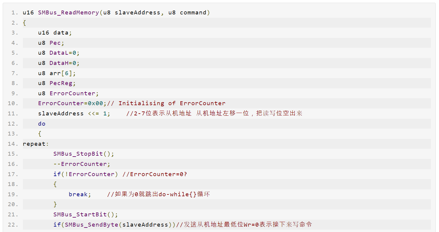
The input parameters for this function are the I2C device's slave address and the command register address. Initially, we shift the slave address left by one bit to make room for the read/write bit, as we are unsure of its initial state. To ensure correctness, we send a stop signal and set ErrorCounter to 0x00. If performing a decrement operation does not result in zero, we proceed with the following steps.
Next, we send a start signal, followed by transmitting the slave device address. Upon successful transmission of the slave address, we continue by sending the command address where the temperature data is stored. Subsequently, we initiate another start signal to begin reading the data. This involves reading the low byte DataL, high byte DataH, and PEC data of the temperature. We then perform PEC data verification by comparing the received PEC data with the calculated PEC data. If they match, we exit the loop. By left shifting the high byte data by 8 bits and performing a bitwise OR operation with the low 8 bits, we obtain the final temperature data.
5.6 Obtaining the Final Temperature Value
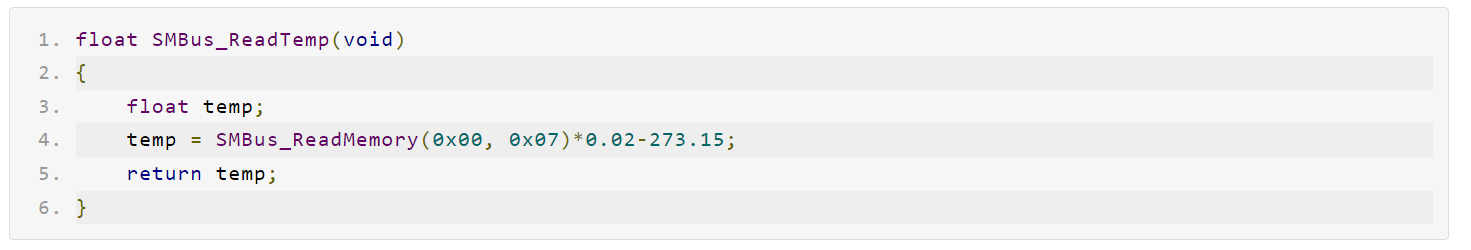
According to the datasheet, we know that by multiplying the final read data by 0.02 and then subtracting 273.15, we will obtain the actual temperature value. This temperature value can then be displayed through serial communication or on an OLED screen, allowing us to visualize the temperature readings from the sensor.
6. CRC-8 Checksum Principle
6.1 Polynomial Division
Polynomial division is similar to arithmetic division, but each bit's division result does not affect other bits, meaning no borrowing occurs to higher-order bits—it essentially is the same as XOR operation. Modular 2 division is applied in calculating cyclic redundancy check (CRC) codes. In CRC checks, two key points must be considered: one is to pre-determine a binary bit string (or polynomial) used as a divisor for both the sender and receiver, which can be randomly selected or follow international standards but must have the highest and lowest bits set as 1; the other is to perform modular 2 division between the original frame and the calculated divisor to obtain the CRC code.
6.2 Specific Steps
Choose a suitable polynomial and determine the divisor.
Observe the number of binary bits in the selected polynomial, then append the data to be sent with an additional (number of bits - 1) of 0s. Proceed to divide the obtained data by the chosen divisor using modular 2 division method, and the remainder obtained will be the CRC checksum. Note that the number of bits in the remainder must be one less than the divisor, i.e., the CRC checksum should have one bit fewer than the divisor, and leading zeros should not be omitted.
6.3 Example 1
Let's assume the polynomial used is: G(X) = X^8 + X^2 + X + 1, and we need to calculate the CRC-8 checksum for 0x1A. Here is the detailed calculation process:
Convert the polynomial into a binary sequence, where G(X) = X^8 + X^2 + X + 1 results in a 9-bit sequence, with bits 8, 2, 1, and 0 being 1, hence the sequence is 100000111.
For the original data to be calculated as 11010 and the polynomial's highest order being 8, append 8 zeroes after the data to become 11010000000000. Perform a modular 2 division using the divisor 100000111. The remainder obtained after division is the desired CRC-8 result.
After the division, the remainder is 0x46, which means the CRC-8 checksum for 0x1A under polynomial G(X) = X^8 + X^2 + X + 1 is 0x46.
6.4 Example 2
Now, let's find out if the CRC-8 checksum for 0xb4 0x07 0xb5 0xd2 0x3a is indeed 0x30:
Convert the polynomial into a binary sequence based on G(X) = X^8 + X^2 + X + 1. Since it has 9 bits, with bits 8, 2, 1, and 0 set to 1, the sequence is 100000111.
For the data to be calculated, b4 07 b5 d2 3a, in binary form:
1011010000000111101101011101001000111010
Append 8 zeroes at the end as the polynomial's highest order is 8, resulting in:
101101000000011110110101110100100011101000000000
Perform a modular 2 division using the divisor 100000111. The remainder obtained is the CRC-8 checksum.
6.5 Reading Temperature Function
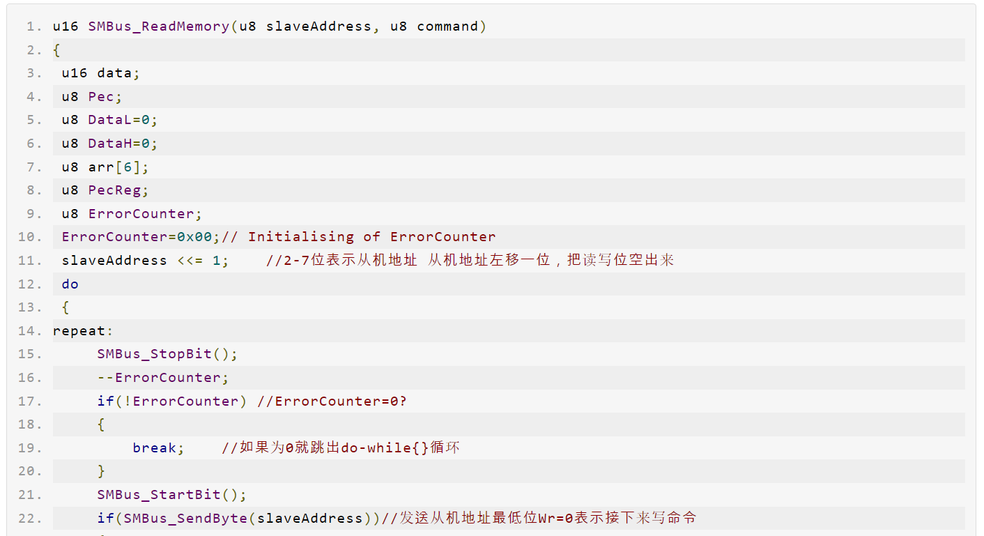
This function takes the I2C device's slave address and command register address as input parameters. Initially, left shift the slave address by one bit to make room for the read/write bit, as the initial state is unknown. To ensure correctness, we send a stop signal when ErrorCounter equals 0x00; then if the result of the decrement operation is not zero, we proceed with the following steps.
Next, send a start signal followed by transmitting the slave device address. If the transmitted slave address is correct, proceed to send the command address within the slave device that stores the temperature data. Subsequently, initiate another start signal to begin reading the data. Read out the low byte DataL, high byte DataH, and PEC data of the temperature. Perform PEC data verification by comparing the read PEC data with the calculated PEC data. If they match, exit the loop. By left shifting the high byte data by 8 bits and performing a bitwise OR operation with the low 8 bits, you will obtain the final data value.
6.6 Obtaining the Final Temperature Value
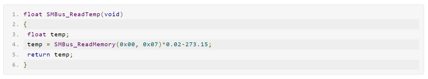
From the datasheet, we know that by multiplying the final read data by 0.02 and subtracting 273.15, we can obtain the actual temperature value. This real temperature value from sensor readings can be obtained by either printing it through serial communication or displaying it on an OLED screen.